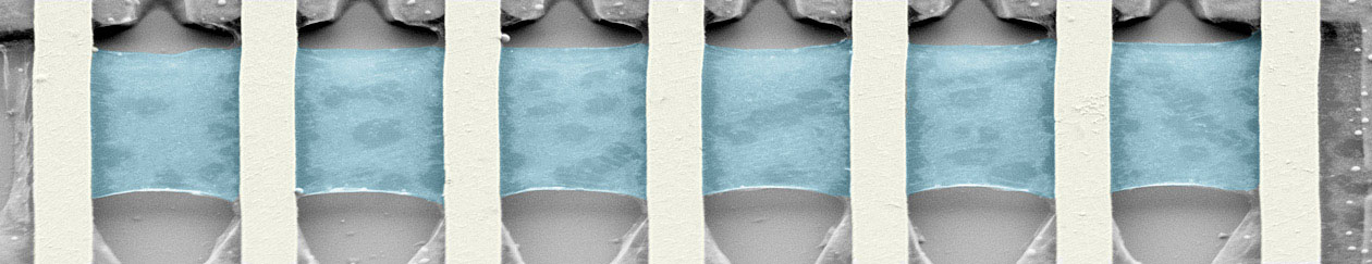
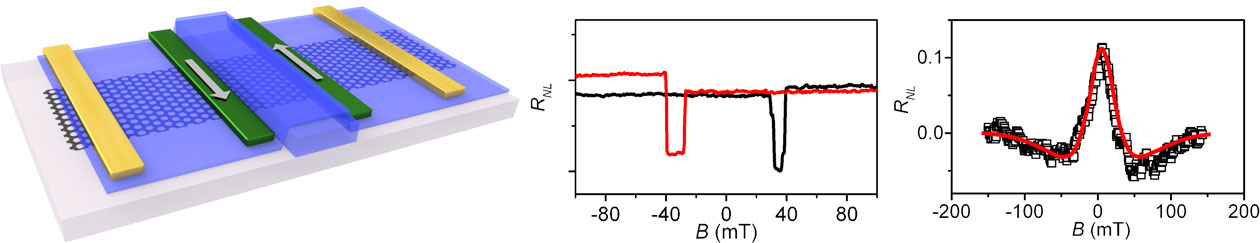
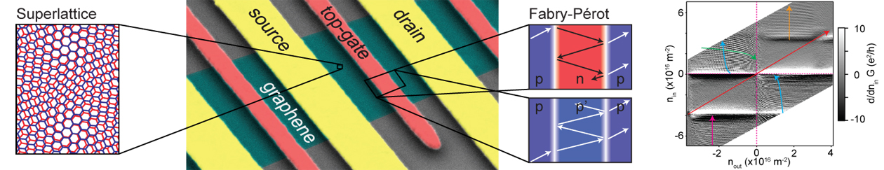
suspended CVD graphene
Masterwork on Quantum Transport in Superconductor Hybrids based on Nanowires
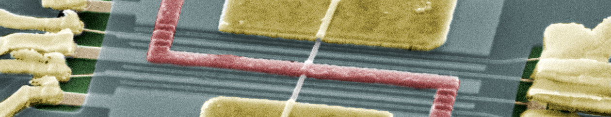
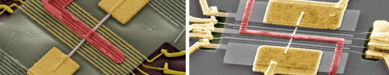
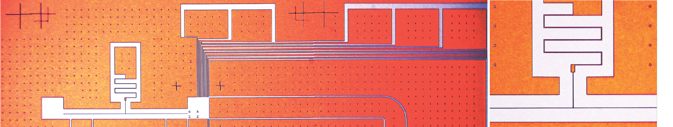
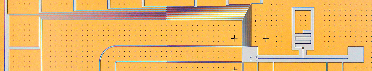
The current project is strongly motivated by the recent excitement about topological phases and Majorana bound states that can appear in hybrid devices in low dimensions, for example in semiconducting nanowires (NWs) with strong spin-orbit coupling, coupled to superconducting contacts. The combination of time-reversal symmetry breaking, spin-orbit field and superconducting pairing can give rise to new states of matter with non-trivial topological phases and unconventional pairing (triplet and p-wave). To unravel the emergence of Majorana bound states in single and coupled NWs, we develop new probes with which the proximity gap and proximity-induced bound states (Andreev-, Shiba states) can be tested. Our approach is based on measuring both DC and AC transport, the latter at GHz frequencies using reflectometry. We are also able to measure microwave radiation in the GHz domain emitted by the quantum device using transmission line resonate circuits providing a deeper insight into charge transport. We are currently deepening our understanding on the proximity effect from an s-wave superconductor into a low dimensional semiconducting NW by studying the evolution of the proximity gap with doping. We are also starting to perform circuit QED experiments with NWs coupled to resonators and we explore the effect of an inhomogeneous magnetic field on quantum dots (QDs) defined in NWs. Furthermore, in a collaboration with Prof. Lucia Sorba from the CNR-Nano we explore InAs QDs with sharp InP barriers that are grown as part of the NWs. These QDs are very promising due to the large confinement potential. We plan to study single and double QDs of this kind coupled to superconductors.
We are looking for a highly motivated student, preferably from the University of Basel, who is keen to explore fundamental aspects of quantum devices. You will design and fabricate your own devices made from semiconducting NWs using state-of-the-art micro- and nanofabrication technologies. Electric measurements will be done down to mK temperatures and include DC to RF techniques based on modern cryogenic circuitry, e.g. rf-resonators. We expect that you have a profound understanding of quantum and solid-state physics as it is taught in a physics curriculum. The specific focus of your particular Master’s project will be defined upon request.
To apply, please email to Christian.Schoenenberger@unibas.ch