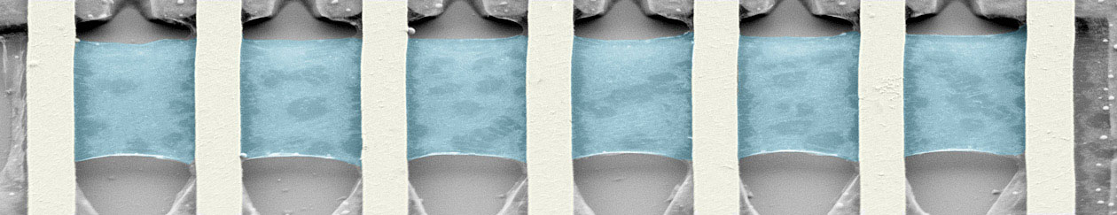
suspended CVD graphene


This projects aims at a single electron pair source which delivers (in principle) on demand pairs of spin-entangled electrons, whereof each electron may leave the device through different arms. While similar photonic EPR sources are widely used in optics in e.g. in teleportation experiments, generating and transporting entanglement in the solid state with electrons is non-trivial due to the strong interaction of the quasiparticles with other particles and excitations. However, in graphene the spin dephasing time now exceeds nanoseconds, yielding a coherent transport distance for spin of impressive 1 mm using the known Fermi velocity of graphene. Hence, entanglement can (in principle) be generated at macroscopic distances beyond millimeters in the solid state.
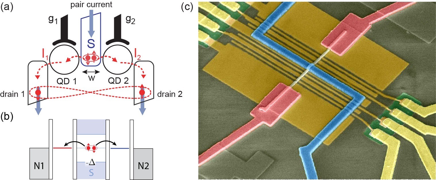
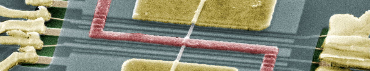
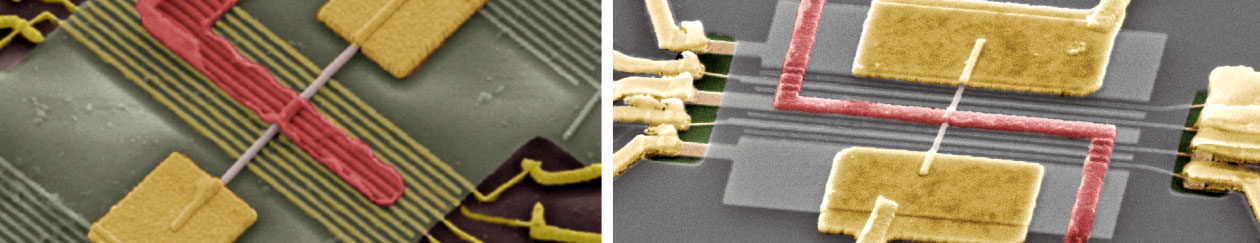
In the current project we start with a Cooper-pair as a naturally spin entangled electron state (in a conventional BCS superconductor the pair is a spin singlet). The device of interest consists of two quantum dots (QDs) tunnel coupled closely together to a central superconductor (see image). Due to interaction effects, which are enhanced in QDs, the “splitting” of the Cooper-pair may become the dominating transport process. In this non-local process, one of the electron tunnels to the left and the other to the right QD. As long as the spin degree is not measured, the states remains entangled. Splitting efficiencies beyond 90% have been realized. We have realized Cooper-pair splitter (CPS) devices in carbon nanotube and semiconducting nanowire based quantum devices and demonstrated large splitting efficiency and to some extend control down to single electron pairs. The devices can also be used to search for Majorana-like bound states as the topology is very much similar.
Current challenges are: better control of individual tunneling rates (in and out tunneling); detection of the entanglement and its life time; manipulation of the singlet state using the quantum toolbox, e.g. electron spin-resonance, detection of a coherent non-local coupling between the two QDs, non-local Andreev bound states.
Funding: ERC-QUEST, SNF
Relevant papers (keyword: CPS):
2025
- High-quality and field resilient microwave resonators on Ge/SiGe quantum well heterostructures
Luigi Ruggiero, Carlo Ciaccia, Pauline Drexler, Vera Jo Weibel, Christian Olsen, Christian Schönenberger, Dominique Bougeard, and Andrea Hofmann.
NPJ Quantum Information (submitted), 2025.
[ Open Data ] [Abstract
  ]
]
Superconducting resonators integrated with germanium (Ge) quantum wells (QWs) offer a promising platform for hybrid quantum devices. Yet, in the most common heterostructure architectures, they have so far been limited by sizable photon losses. Here, we report the fabrication and characterization of microwave resonators patterned in the aluminum (Al) thin film of an in-situ grown superconductor/semiconductor hybrid heterostructure (HS). The semiconductor part of this hybrid HS is grown on a commercial Ge substrate. We consistently achieve internal quality factors Qi > 1000, surpassing previous results on Ge QW heterostructures grown using the concept of a virtual Ge substrate on silicon (Si) substrates. We reach Qi approx. 49’000 at single-photon occupation and a plateau of Qi approx. 20’000 at sub-one photon, an order of magnitude larger than any previously reported value of resonators on Ge QW structures at low power. We further characterize the thin Al film forming the resonator, extracting its kinetic inductance and superconducting gap, and studying its magnetic field dependence. Notably, the resonance remains well-defined up to in-plane magnetic fields of 850 mT. A hysteresis emerges in the out-of-plane magnetic field dependence, for both the resonance frequency and the quality factor, indicating an interesting interplay between vortex-and quasiparticle loss mechanisms.
- Radio-Frequency Detection of Fabry–Pérot Interference and Quantum Capacitance in Long-Channel Three-Dimensional Dirac Semimetal Cd3As2 Nanowires
Sung Jin An, Jisu Kim, Myung-Chul Jung, Kidong Park, Jeunghee Park, Seung-Bo Shim, Hakseong Kim, Zhuo Bin Siu, Mansoor B. A. Jalil, Christian Schönenberger, Nojoon Myoung, Jungpil Seo, and Minkyung Jung.
ACS Appl. Elec. Mat., 2025.
[arXiv:2509.16934 ] [ Open Data ] [Abstract ]
We demonstrate phase-coherent transport in suspended long-channel Cd3As2 nanowire devices using both direct current (DC) transport and radiofrequency (RF) reflectometry measurements. By integrating Cd3As2 nanowires with on-chip superconducting LC resonators, we achieve sensitive detection of both resistance and quantum capacitance variations. In a long-channel device (L ≈ 1.8 μm), clear Fabry–Pérot (FP) interference patterns are observed in both DC and RF measurements, providing strong evidence for ballistic electron transport. RF reflectometry reveals gate-dependent modulations of the resonance frequency arising from quantum capacitance oscillations induced by changes in the density of states and FP interference. These oscillations exhibit a quasi-periodic structure that closely correlates with the FP patterns in DC transport measurements. In another device of a Cd3As2 nanowire Josephson junction (L ≈ 730 nm, superconducting Al contacts), FP interference patterns are too weak to be resolved in DC conductance but are detectable using RF reflectometry. These results demonstrate the high quality of our Cd3As2 nanowires and the versatility of RF reflectometry, establishing their potential for applications in topological quantum devices such as Andreev qubits or gatemon architectures.
- Gate-tunable double-dome superconductivity in twisted trilayer graphene
Zekang Zhou, Jin Jiang, Paritosh Karnatak, Ziwei Wang, Glenn Wagner, Kenji Watanabe, Takashi Taniguchi, Christian Schönenberger, S. A. Parameswaran, Steven H. Simon, and Mitali Banerjee.
Nature Phys. 21, 1773-1779, 2025.
[arXiv:2404.09909] [Abstract ]
Graphene moiré systems are ideal environments for investigating complex phase diagrams and gaining fundamental insights into the mechanisms that underlie them, as they permit controlled manipulation of electronic properties. Magic-angle twisted trilayer graphene has emerged as a key platform for exploring moiré superconductivity due to the robustness of its superconducting order and the ability to tune its energy bands with an electric field. Here we report the direct observation of two domes of superconductivity in the phase diagram of magic-angle twisted trilayer graphene. The dependence of the superconductivity of doped holes on the temperature, magnetic field and bias current shows that it is suppressed near a specific filling of the moiré flat band, leading to a double dome in the phase diagram within a finite range of the displacement field. The transport properties are also indicative of a phase transition and the potentially distinct nature of superconductivity in the two domes. Hartree–Fock calculations incorporating mild strain yield an incommensurate Kekulé spiral state whose effective spin polarization peaks in the regime where superconductivity is suppressed in the experiments.
- A coherence sweet spot with enhanced dipolar coupling
J. H. Ungerer, A. Pally, S. Bosco, A. Kononov, D. Sarmah, S. Lehmann, C. Thelander, V. F. Maisi, P. Scarlino, D. Loss, A. Baumgartner, and C. Schönenberger.
Comm. Physics 8, 2025.
[arXiv:2405.10796] [ Open Data ] [Abstract ]
Qubits require a compromise between operation speed and coherence. Here, we demonstrate a compromise-free singlet-triplet (ST) qubit, where the qubit couples maximally to the driving field while simultaneously coupling minimally to the dominant noise sources. The qubit is implemented in a crystal-phase defined double-quantum dot in an InAs nanowire. Using a superconducting resonator, we measure the spin-orbit interaction (SOI) gap, the spin-photon coupling strength and the qubit decoherence rate as a function of the in-plane magnetic-field orientation. We demonstrate a spin qubit sweet spot maximizing the dipolar coupling and simultaneously minimizing the decoherence. Our theoretical description postulates phonons as the most likely dominant noise source. The compromise-free sweet spot originates from the SOI suggesting that it is not restricted to this material platform, but might find applications in any material with SOI. These findings pave the way for enhanced engineering of these nanomaterials for next-generation qubit technologies.
- Entangled photon-pair emission in circuit QED from a Cooper pair splitter
Michele Governale, Christian Schönenberger, Pasquale Scarlino, and Gianluca Rastelli.
Phys. Rev. X Quantum 6, 20339, 2025.
[arXiv:2407.15109] [ Open Data ] [Abstract ]
As a waveguide circuit QED architecture, we investigate theoretically the single-photon pair emission of a Cooper pair splitter composed of two double quantum dots, each coupled to a microwave transmission line. We find that this system can generate frequency-entangled photon pairs in the left and right transmission lines, specifically a superposition of two photon wave packets at different frequencies. The frequency entanglement of the two photons arises from the particle-hole coherent superposition (i.e., Andreev bound states) involving the delocalized entangled spin singlet. We also estimate a lower bound for the efficiency of entangled photon-pair generation, accounting for the presence of nonradiative processes such as phonon emissions. Our proposal is realistic and achievable with state-of-the-art techniques in quantum microwave engineering with electostatically defined semiconducting quantum dots.
- Large tunable kinetic inductance in a twisted graphene superconductor
R. Jah, M. Endres, K. Watanabe, T. Taniguchi, M. Banerje, C. Schönenberger, and P. Karnatak.
Phys. Rev. Lett. 134, 216001, 2025.
[arXiv:2403.02320] [ Open Data ] [Abstract ]
Twisted graphene based moir\´e heterostructures host a flat band at the magic angles where the kinetic energy of the charge carriers is quenched and interaction effects dominate. This results in emergent phases such as superconductors and correlated insulators that are electrostatically tunable. We investigate superconductivity in twisted trilayer graphene (TTG) by integrating it as the weak link in a superconducting quantum interference device (SQUID). The measured current phase relation (CPR) yields a large and tunable kinetic inductance, up to 150 nH per square, of the electron and hole-type intrinsic superconductors. We further show that the specific kinetic inductance and the critical current density are universally related via the superconducting coherence length, and extract an upper bound of ∼ 200 nm for the coherence length. We discuss the implications of a large coherence length in twisted graphene superconductors.
- Andreev-Qubit-Qubit-Kopplung auf Distanz
C. Schönenberger.
Physik in unserer eit 56, 60-61, 2025.
[Abstract]
Mikroskopische Andreev-Qubits lassen sich nun kohärent über makroskopische Distanzen koppeln, was die Erzeugung von verschränkten Zuständen und allgemeinen Zwei-Qubit-Operationen ermöglicht. Dies konnte kürzlich sowohl für Andreev-Paar-Qubits als auch für Andreev-Spin-Qubits demonstriert werden
- ‘Unconventional’ Superconductivity probed in twisted graphene
Paritosh Karnatak and Christian Schönenberger.
Nature (News & Views) 638, 44-45, 2025.
2024
- Decoherence in a crystal-phase defined double quantum dot charge qubit strongly coupled to a high-impedance resonator
A. Ranni, S. Haldar, H. Havir, S. Lehman, P. Scarlino, A. Baumgartner, C. Schönenberger, C. Thelander, K. Dick, P. P. Potts, and V. F. Maisi.
Physical Review Research 6, 43134, 2024.
[arXiv:2308.14887v1] [Abstract ]
Decoherence of a charge qubit is usually credited to charge noise in the environment. Here we show that charge noise may not be the limiting factor for the qubit coherence. To this end, we study coherence properties of a crystal-phase defined semiconductor nanowire double quantum dot (DQD) charge qubit strongly coupled to a high-impedance resonator using radio-frequency reflectometry. Response of this hybrid system is measured both at a charge noise sensitive operation point (with finite DQD detuning) and at an insensitive point (so-called sweet spot with zero detuning). A theoretical model based on the Jaynes-Cummings Hamiltonian matches the experimental results well and yields only a 10\% difference in decoherence rates between the two cases, despite that the sensitivity to detuning charge noise differs by a factor of 5. Therefore, the charge noise is not limiting the coherence in this experiment with this type of semiconducting nanowire qubits.
- Photon-mediated long-range coupling of two Andreev pair qubits
L. Y. Cheung, R. Haller, A. Kononov, C. Ciaccia, J. H. Ungerer, T. Kanne, J. Nygård, P. Winkel, T. Reisinger, I. M. Pop, A. Baumgartner, and C. Schönenberger.
Nature Physics 20, 1793–1797, 2024.
[arXiv:2310.15995] [ Open Data ] [Abstract ]
When two superconductors are separated by a weak link, a supercurrent is carried by Andreev bound states formed by the phase-coherent reflection of electrons and their time-reversed partners. The two levels associated with a single, highly transmissive Andreev bound state can serve as a qubit due to the potentially large energy difference with the next bound state. Although coherent manipulation of these so-called Andreev pair qubits has been demonstrated, long-range qubit–qubit coupling, which is necessary for advanced quantum computing architectures, has not yet been achieved. Here, we demonstrate coherent remote coupling between two Andreev pair qubits mediated by a microwave photon in a superconducting cavity coupler. The latter hosts two modes that are engineered to have very different coupling rates to an external port. The strongly coupled mode can be used to perform a fast read-out of each qubit, while we use the weakly coupled mode to mediate the coupling between the qubits. When both qubits are tuned into resonance with the latter mode, we find excitation spectra with characteristic avoided crossings. We identify two-qubit states that are entangled over a distance of 6 mm. This work establishes Andreev pair qubits as a compact and scalable approach to developing quantum computers
- Electron wave and quantum optics in graphene
Himadri Chakraborti, Cosimo Gorini, Angelika Knothe, Ming-Hao Liu, Peter Makk, Francois D. Parmentier, David Perconte, Klaus Richter, Preden Roulleau, Christian Schönenberger Benjamin Sacépé, and Wenmin Yang.
Journal of Physics: Condensed Matter 36, 2024.
[arXiv:2401.04233] [Abstract ]
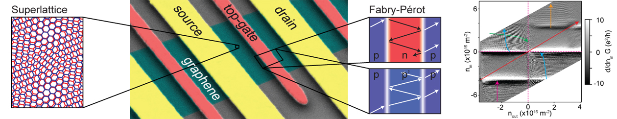
In the last decade, graphene has become an exciting platform for electron optical experiments, in some aspects superior to conventional twodimensional electron gases (2DEGs). A major advantage, besides the ultra-large mobilities, is the fine control over the electrostatics, which gives the possibility of realising gap-less and compact p-n interfaces with high precision. The latter host non-trivial states, e.g. , snake states in moderate magnetic fields, and serve as building blocks of complex electron interferometers. Thanks to the Dirac spectrum and its non-trivial Berry phase, the internal (valley and sublattice) degrees of freedom, and the possibility to tailor the band structure using proximity effects, such interferometers open up a completely new playground based on novel device architectures. In this review, we introduce the theoretical background of graphene electron optics, fabrication methods used to realise electron-optical devices, and techniques for corresponding numerical simulations. Based on this, we give a comprehensive review of ballistic transport experiments and simple building blocks of electron optical devices both in single and bilayer graphene, highlighting the novel physics that is brought in compared to conventional 2DEGs. After describing the different magnetic field regimes in graphene p-n junctions and nanostructures, we conclude by discussing the state of the art in graphene-based Mach-Zender and Fabry-Perot interferometers.
- Coherent control of a few-channel hole type gatemon qubit
H. Zheng, L. Y. Cheung, N. Sangwan, A. Kononov, R. Haller, J. Ridderbos, C. Ciaccia, J. H. Ungerer, A. Li, E. P. A. M. Bakkers, A. Baumgartner, and C. Schönenberger.
Nano Lett. 24, 7173, 2024.
[arXiv:2312.06411] [ Open Data ] [Abstract ]
Gatemon qubits are the electrically tunable cousins of superconducting transmon qubits. In this work, we demonstrate the full coherent control of a gatemon qubit based on hole carriers in a Ge/Si core/shell nanowire, with the longest coherence times in group IV material gatemons to date. The key to these results is a high-quality Josephson junction obtained in a straightforward and reproducible annealing technique. We demonstrate that the transport through the narrow junctions is dominated by only two quantum channels, with transparencies up to unity. This novel qubit platform holds great promise for quantum information applications, not only because it incorporates technologically relevant materials, but also because it provides new opportunities, like an ultrastrong spin-orbit coupling in the few-channel regime of Josephson junctions.
- Strong coupling between a microwave photon and a singlet-triplet qubit
J. H. Ungerer, A. Pally, A. Kononov, S. Lehmann, J. Ridderbos, C. Thelander, K. A. Dick, V. F. Maisi, P. Scarlino, A. Baumgartner, and C. Schönenberger.
Nature Communications 15, 1068, 2024.
[arXiv:2303.16825] [ Open Data ] [Abstract ]
Tremendous progress in few-qubit quantum processing has been achieved lately using superconducting resonators coupled to gate voltage defined quantum dots. While the strong coupling regime has been demonstrated recently for odd charge parity flopping mode spin qubits, first attempts towards coupling a resonator to even charge parity singlet-triplet spin qubits have resulted only in weak spin-photon coupling strengths. Here, we integrate a zincblende InAs nanowire double quantum dot with strong spin-orbit interaction in a magnetic-field resilient, high-quality resonator. In contrast to conventional strategies, the quantum confinement is achieved using deterministically grown wurtzite tunnel barriers without resorting to electrical gating. Our experiments on even charge parity states and at large magnetic fields, allow us to identify the relevant spin states and to measure the spin decoherence rates and spin-photon coupling strengths. Most importantly, at a specific magnetic field, we find an anti-crossing between the resonator mode in the single photon limit and a singlet-triplet qubit with an electron spin-photon coupling strength of $g = 114 \pm 9$ MHz, reaching the strong coupling regime in which the coherent coupling exceeds the combined qubit and resonator linewidth.
- Charge-4e supercurrent in an InAs-Al superconductor-semiconductor heterostructure
C. Ciaccia, R. Haller, A. C. C. Drachmann, T. Lindemann, M. J. Manfra, and Schrade C. C. Schönenberger.
Communication Physics 7, 41, 2024.
[arXiv:2306.05467] [ Open Data ] [Abstract ]
Superconducting qubits with intrinsic noise protection offer a promising approach to improve the coherence of quantum information. Crucial to such protected qubits is the encoding of the logical quantum states into wavefunctions with disjoint support. Such encoding can be achieved by a Josephson element with an unusual charge-4e supercurrent emerging from the coherent transfer of pairs of Cooper-pairs. In this work, we demonstrate the controlled conversion of a conventional charge-2e dominated to a charge-4e dominated supercurrent in a superconducting quantum interference device (SQUID) consisting of gate-tunable planar Josephson junctions (JJs). We investigate the ac Josephson effect of the SQUID and measure a dominant photon emission at twice the fundamental Josephson frequency together with a doubling of the number of Shapiro steps, both consistent with the appearance of charge-4e supercurrent. Our results present a step towards novel protected superconducting qubits based on superconductor-semiconductor hybrid materials.
2023
- Performance of high impedance resonators in dirty dielectric environments
J. H. Ungerer, D. Sarmah, A. Kononov, J. Ridderbos, R. Haller, Yi L. Cheung, and C. Schönenberger.
EPJ Quantum Technology 10, 2023.
[arXiv:2302.06303] [ Open Data ] [Abstract ]
High-impedance resonators are a promising contender for realizing long-distance entangling gates between spin qubits. Often, the fabrication of spin qubits relies on the use of gate dielectrics which are detrimental to the quality of the resonator. Here, we investigate loss mechanisms of high-impedance NbTiN resonators in the vicinity of thermally grown SiO2 and Al2O3 fabricated by atomic layer deposition. We benchmark the resonator performance in elevated magnetic fields and at elevated temperatures and find that the internal quality factors are limited by the coupling between the resonator and two-level systems of the employed oxides. Nonetheless, the internal quality factors of high-impedance resonators exceed 103 in all investigated oxide configurations which implies that the dielectric configuration would not limit the performance of resonators integrated in a spin-qubit device. Because these oxides are commonly used for spin qubit device fabrication, our results allow for straightforward integration of high-impedance resonators into spin-based quantum processors. Hence, these experiments pave the way for large-scale, spin-based quantum computers.
- AC Josephson effect in a gate-tunable Cd3As2 nanowire superconducting weak link
R. Haller, M. Osterwalder, G. Fülöp, J. Ridderbos, M. Jung, and C. Schönenberger.
Phys. Rev. B 108, 94514, 2023.
[arXiv:2305.19996] [ Open Data ] [Abstract ]
Three-dimensional topological Dirac semimetals have recently gained significant attention, since they possess exotic quantum states. When constructing Josephson junctions utilizing these materials as the weak link, the fractional ac Josephson effect emerges in the presence of a topological supercurrent contribution. We investigate the ac Josephson effect in a Dirac semimetal Cd3As2 nanowire using two complementary methods: by probing the radiation spectrum and by measuring Shapiro patterns. With both techniques, we find that conventional supercurrent dominates at all investigated doping levels and that any potentially present topological contribution falls below our detection threshold. The inclusion of thermal noise in a resistively and capacitively shunted junction (RCSJ) model allows us to reproduce the microwave characteristics of the junction. With this refinement, we explain how weak superconducting features can be masked and provide a framework to account for elevated electronic temperatures present in realistic experimental scenarios.
- Edge Contacts to Atomically Precise Graphene Nanoribbons
W. Huang, O. Braun, D. I. Indolese, G. B. Barin, G. Gandus, M. Stiefel, A. Olziersky, K. Müllen, M. Luisier, D. Passerone, P. Ruffieux, C. Schönenberger, K. Watanabe, T. Taniguchi, R. Fasel, J. Zhang, M. Calame, and M. L. Perrin.
ACS Nano 17, 18706, 2023.
[Abstract]
Bottom-up-synthesized graphene nanoribbons (GNRs) are an emerging class of designer quantum materials that possess superior properties, including atomically controlled uniformity and chemically tunable electronic properties. GNR-based devices are promising candidates for next-generation electronic, spintronic, and thermoelectric applications. However, due to their extremely small size, making electrical contact with GNRs remains a major challenge. Currently, the most commonly used methods are top metallic electrodes and bottom graphene electrodes, but for both, the contact resistance is expected to scale with overlap area. Here, we develop metallic edge contacts to contact nine-atom-wide armchair GNRs (9-AGNRs) after encapsulation in hexagonal boron-nitride (h-BN), resulting in ultrashort contact lengths. We find that charge transport in our devices occurs via two different mechanisms: at low temperatures (9 K), charges flow through single GNRs, resulting in quantum dot (QD) behavior with well-defined Coulomb diamonds (CDs), with addition energies in the range of 16 to 400 meV. For temperatures above 100 K, a combination of temperature-activated hopping and polaron-assisted tunneling takes over, with charges being able to flow through a network of 9-AGNRs across distances significantly exceeding the length of individual GNRs. At room temperature, our short-channel field-effect transistor devices exhibit on/off ratios as high as 3 × 10⁵ with on-state current up to 50 nA at 0.2 V. Moreover, we find that the contact performance of our edge-contact devices is comparable to that of top/bottom contact geometries but with a significantly reduced footprint. Overall, our work demonstrates that 9-AGNRs can be contacted at their ends in ultra-short-channel FET devices while being encapsulated in h-BN.
- Gate Tunable Josephson Diode in Proximitized InAs Supercurrent Interferometers
C. Ciaccia, R. Haller, A. C. C. Drachmann, T. Lindemann, M. J. Manfra, C. Schrade, and C. Schönenberger.
Phys. Rev. Research 5, 33131, 2023.
[arXiv:2304.00484] [ Open Data ] [Abstract ]
The Josephson diode (JD) is a non-reciprocal circuit element that supports a larger critical current in one direction compared to the other. This effect has gained a growing interest because of promising applications in superconducting electronic circuits with low power consumption. Some implementations of a JD rely on breaking the inversion symmetry in the material used to realize Josephson junctions (JJs), but a recent theoretical proposal has suggested that the effect can also be engineered by combining two JJs hosting highly transmitting Andreev bound states in a Superconducting Quantum Interference Device (SQUID) at a small, but finite flux bias~[1]. We realized a SQUID with two JJs fabricated in a proximitized InAs two-dimensional electron gas (2DEG). We demonstrate gate control of the diode efficiency from zero up to around $30$\% for different flux biases which comes close to the maximum of $\sim 40$\% predicated in Ref.~\cite{Souto2022}. The key ingredient to the JD effect in the SQUID arrangement is the presence of an asymmetry between the two SQUID arms.
- Charge-sensing of a Ge/Si core/shell nanowire double quantum dot using a high-impedance superconducting resonator
J. H. Ungerer, Chevalier P. Kwon, T. Patlatiuk, J. Ridderbos, A. Kononov, D. Sarmah, E. P. A. M. Bakkers, D. Zumbühl, and C. Schönenberger.
Materials for Quantum Technologies 3, 31001, 2023.
[arXiv:2211.00763] [ Open Data ] [Abstract ]
Spin qubits in germanium are a promising contender for scalable quantum computers. Reading out of the spin and charge configuration of quantum dots formed in Ge/Si core/shell nanowires is typically performed by measuring the current through the nanowire. Here, we demonstrate a more versatile approach on investigating the charge configuration of these quantum dots. We employ a high-impedance, magnetic-field resilient superconducting resonator based on NbTiN and couple it to a double quantum dot in a Ge/Si nanowire. This allows us to dispersively detect charging effects, even in the regime where the nanowire is fully pinched off and no direct current is present. Furthermore, by increasing the electro-chemical potential far beyond the nanowire pinch-off, we observe indications for depleting the last hole in the quantum dot by using the second quantum dot as a charge sensor. This work opens the door for dispersive readout and future spin-photon coupling in this system
- Intermediate states in Andreev bound state fusion
C. Jünger, S. Lehmann, K. A. Dick, C. Thelander, C. Schönenberger, and A. Baumgartner.
Communication Physics 6, 2023.
[arXiv:2111.00651] [ Open Data ] [Abstract ]
Hybridization is a very fundamental quantum mechanical phenomenon, with the text book example of binding two hydrogen atoms in a hydrogen molecule. In semiconductor physics, a quantum dot (QD) can be considered as an artificial atom, with two coupled QDs forming a molecular state, and two electrons on a single QD the equivalent of a helium atom. Here, we report tunnel spectroscopy experiments illustrating the hybridisation of another type of discrete quantum states, namely of superconducting subgap states that form in segments of a semiconducting nanowire in contact with superconducting reservoirs. We show and explain a collection of intermediate states found in the process of merging individual bound states, hybridizing with a central QD and eventually coherently linking the reservoirs. These results may serve as a guide in future Majorana fusion experiments and explain a large variety of recent bound state experiments.
- Current-phase relation of WTe2 Josephson junctions
M. Endres, A. Kononov, H. S. Arachchige, Jiaqiang Yan, D. Mandrus, K. Watanabe, T. Taniguchi, and C. Schönenberger.
Nano Letters 23, 4654-4659, 2023.
[arXiv:2211.10273] [ Open Data ] [Abstract ]
When a topological insulator is incorporated into a Josephson junction, the system is predicted to reveal the fractional Josephson effect with a 4$\pi$-periodic current-phase relation. Here, we report the measurement of a $4\pi$-periodic switching current through an asymmetric SQUID, formed by the higher-order topological insulator WTe$_2$. Contrary to the established opinion, we show that a high asymmetry in critical current and negligible loop inductance are not sufficient by themselves to reliably measure the current-phase relation. Instead, we find that our measurement is heavily influenced by additional inductances originating from the self-formed PdTe$_{\text{x}}$ inside the junction. We therefore develop a method to numerically recover the current-phase relation of the system and find the $1.5\,\mu \text{m}$ long junction to be best described in the short ballistic limit. Our results highlight the complexity of subtle inductance effects that can give rise to misleading topological signatures in transport measurements.
- Origin of subgap states in normal-insulator-superconductor van der Waals heterostructures
P. Karnatak, Z. Mingazheva, K. Watanabe, T. Taniguchi, H. Berger, L. Forró, and C. Schönenberger.
Nano Letters 23, 2454–2459, 2023.
[arXiv:2207.05741] [ Open Data ] [Abstract ]
Superconductivity in van der Waals materials, such as NbSe2 and TaS2, is fundamentally novel due to the effects of dimensionality, crystal symmetries, and strong spin-orbit coupling. In this work we perform tunnel spectroscopy on NbSe2 by utilizing MoS2 or hexagonal Boron Nitride (hBN) as a tunnel barrier. We observe subgap excitations and probe their origin by studying various heterostructure designs. We show that the edge of NbSe2 hosts many defect states, which strongly couple to the superconductor and form Andreev bound states. Furthermore, by isolating the NbSe2 edge we show that the subgap states are ubiquitous in MoS2 tunnel barriers, but absent in hBN tunnel barriers, suggesting defects in MoS2 as their origin. Their magnetic nature reveals a singlet or a doublet type ground state and based on nearly vanishing g-factors or avoided-crossing of subgap excitations we highlight the role of strong spin-orbit coupling.
2022
- Spin Cross-Correlation Experiments in an Electron Entangler
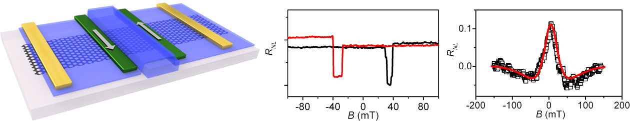
A. Bordoloi, V. Zannier, L. Sorba, C. Schönenberger, and A. Baumgartner.
Nature 612, 454-458, 2022.
[arXiv:2203.07970] [ Open Data ] [Abstract ]
Correlations are fundamental in describing many body systems – not only in natural sciences. However, in experiments, correlations are notoriously difficult to assess on the microscopic scale, especially for electron spins. Here, we demonstrate a direct measurement of the spin cross-correlations between the currents of a Cooper pair splitter, an electronic device that emits electrons originating from Cooper pairs in a superconductor. While it is firmly established theoretically that these electron pairs form maximally spin-entangled singlet states with opposite spin projections, no spin correlation experiments have been demonstrated so far. We use ferromagnetic sidegates, compatible with superconducting electronic structures, to individually spin polarize the transmissions of two quantum dots fabricated in the two electronic paths, which act as tunable spin filters. The signals are detected in standard transport and in highly sensitive transconductance experiments. We find that the spin-cross correlation is negative, compatible with spin singlet emission, and deviates from the ideal value mostly due to a finite overlap of the Zeeman split quantum dot states. Our results demonstrate a new route to perform spin auto- and cross correlation experiments in nanometer scaled electronic devices, especially suitable for those relying on magnetic field sensitive superconducting elements, like unconventional, triplet or topologically non-trivial superconductors, or to perform Bell tests with massive particles, like electrons.
- Impact of the gate geometry on adiabatic charge pumping in InAs double quantum dots
Sung Jin An, Myung-Ho Bae, Myoung-Jae Lee, Man Suk Song, Jesper Nygård, Christian Schönenberger, Andreas Baumgartner, Jungpil Seo, and Minkyung Jung.
Nanoscale Adv. 4, 3816-3823, 2022.
[Abstract]
We compare the adiabatic quantized charge pumping performed in two types of InAs nanowire double quantum dots (DQDs), either with tunnel barriers defined by closely spaced narrow bottom gates, or by well-separated side gates. In the device with an array of bottom gates of 100 nm pitch and 10 μm lengths, the pump current is quantized only up to frequencies of a few MHz due to the strong capacitive coupling between the bottom gates. In contrast, in devices with well-separated side gates with reduced mutual gate capacitances, we find well-defined pump currents up to 30 MHz. Our experiments demonstrate that high frequency quantized charge pumping requires a careful optimization of the device geometry, including the typically neglected gate feed lines.
- Transparent Josephson Junctions in Higher-Order Topological Insulator WTe2 via Pd Diffusion
M. Endres, A. Kononov, M. Stiefel, M. Wyss, H. S. Arachchige, Jiaqiang Yan, D. Mandrus, K. Watanabe, T. Taniguchi, and C. Schönenberger.
Phys. Rev. Mat. 6, L081201, 2022.
[arXiv:2205.06542] [ Open Data ] [Abstract ]
Highly transparent superconducting contacts to a topological insulator (TI) remain a persistent challenge on the route to engineer topological superconductivity. Recently, the higher-order TI WTe2 was shown to turn superconducting when placed on palladium (Pd) bottom contacts, demonstrating a promising material system in perusing this goal. Here, we report the diffusion of Pd into WTe2 and the formation of superconducting PdTex as the origin of observed superconductivity. We find an atomically sharp interface between the diffusion layer and its host crystal, forming state-of-the-art superconducting contacts to a TI. The diffusion is discovered to be non-uniform along the width of the WTe2 crystal, with a greater extend along the edges compared to the bulk. The potential of this contacting method is highlighted in transport measurements on Josephson junctions by employing external superconducting leads.
- From Cooper pair splitting to the nonlocal spectroscopy of a Shiba state
Z. Scherübl, G. Fülöp, J. Gramich, A. Pályi, C. Schönenberger, J. Nygard, and S. Csonka.
Phys. Rev. Research 4, 23143, 2022.
[arXiv:2108.12155] [ Open Data ] [Abstract ]
Cooper pair splitting (CPS) is a way to create spatially separated, entangled electron pairs. To this day, CPS is often identified in experiments as a spatial current correlation. However, such correlations can arise even in the absence of CPS, when a quantum dot is strongly coupled to the superconductor, and a subgap Shiba state is formed. Here, we present a detailed experimental characterization of those spatial current correlations, as the tunnel barrier strength between the quantum dot and the neighboring normal electrode is tuned. The correlation of the non-local signal and the barrier strength reveals a competition between CPS and the non-local probing of the Shiba state. We describe our experiment with a simple transport model, and obtain the tunnel couplings of our device by fitting the model’s prediction to the measured conductance correlation curve. Furthermore, we use our theory to extract the contribution of CPS to the non-local signal.
- 2D materials shrink superconducting qubits
C. Schönenberger.
Nature Materials (News & Views) 21, 381, 2022.
[Abstract]
The exceptional quality of hexagonal boron nitride crystals that can be cleaved into few layers provides ultrathin dielectrics, thereby opening a route to ultrasmall capacitors with large capacitances. With such capacitors, the superconducting transmon qubit is scaled down by orders of magnitude. % Associated Content: `Hexagonal boron nitride as a low-loss dielectric for superconducting quantum circuits and qubits’ by J. J.-I. Wang et al. Nature Materials 21, 398–403 (2022)
- Phase-dependent microwave response of a graphene Josephson junction
R. Haller, G. Fülöp, D. Indolese, J. Ridderbos, R. Kraft, Luk Yi Cheung, J. H. Ungerer, K. Watanabe, T. Taniguchi, D. Beckmann, R. Danneau, P. Virtanen, and C. Schönenberger.
Phys. Rev. Research 4, 13198, 2022.
[arXiv:2108.00989] [ Open Data ] [Abstract ]
Gate-tunable Josephson junctions embedded in a microwave environment provide a promising platform to in-situ engineer and optimize novel superconducting quantum circuits. The key quantity for the circuit design is the phase-dependent complex admittance of the junction, which can be probed by sensing an rf SQUID with a tank circuit. Here, we investigate a graphene-based Josephson junction as a prototype gate-tunable element enclosed in a SQUID loop that is inductively coupled to a superconducting resonator operating at 3 GHz. With a concise circuit model that describes the dispersive and dissipative response of the coupled system, we extract the phase-dependent junction admittance corrected for self-screening of the SQUID loop. We decompose the admittance into the current-phase relation and the phase-dependent loss and as these quantities are dictated by the spectrum and population dynamics of the supercurrent-carrying Andreev bound states, we gain insight to the underlying microscopic transport mechanisms in the junction. We theoretically reproduce the experimental results by considering a short, diffusive junction model that takes into account the interaction between the Andreev spectrum and the electromagnetic environment, from which we deduce a lifetime of ~17 ps for non-equilibrium populations.
- Magnetic, thermal, and topographic imaging with a nanometer-scale SQUID-on-cantilever scanning probe
M. Wyss, K. Bagani, D. Jetter, E. Marchiori, A. Vervelaki, B. Gross, J. Ridderbos, S. Gliga, C. Schönenberger, and M. Poggio.
Phys. Rev. Appl. 17, 34002, 2022.
[arXiv:2109.06774] [Abstract ]
Scanning superconducting quantum interference device (SQUID) microscopy is a magnetic imaging technique combining high field sensitivity with nanometer-scale spatial resolution. State-of-the-art SQUID-on-tip probes are now playing an important role in mapping correlation phenomena, such as superconductivity and magnetism, which have recently been observed in two-dimensional van der Waals materials. Here, we demonstrate a scanning probe that combines the magnetic and thermal imaging provided by an on-tip SQUID with the tip-sample distance control and topographic contrast of a non-contact atomic force microscope (AFM).We pattern the nanometer-scale SQUID, including its weak-link Josephson junctions, via focused ion beam milling at the apex of a cantilever coated with Nb, yielding a sensor with an effective diameter of 365 nm, field sensitivity of 9.5 nT / sqrt(Hz)and thermal sensitivity of 620 nK / sqrt(Hz)operating in magnetic fields up to 1.0 T. The resulting SQUID-on-lever is a robust AFM-like scanning probe that expands the reach of sensitive nanometerscale magnetic and thermal imaging beyond what is currently possible.
2021
- Spectroscopy of the local density-of-states in nanowires using integrated quantum dots
F. S. Thomas, M. Nilsson, C. Ciaccia, C. Jünger, F. Rossi, V. Zannier, L. Sorba, A. Baumgartner, and C. Schönenberger.
Phys. Rev. B 104, 115415, 2021.
[arXiv:2105.10910] [ Open Data ] [Abstract ]
In quantum dot (QD) electron transport experiments additional features can appear in the differential conductance dI/dV that do not originate from discrete states in the QD, but rather from a modulation of the density-of-states (DOS) in the leads. These features are particularly pronounced when the leads are strongly confined low dimensional systems, such as in a nanowire (NW) where transport is one-dimensional and quasi-zero dimensional lead-states can emerge. In this paper we study such lead-states in InAs NWs. We use a QD integrated directly into the NW during the epitaxial growth as an energetically and spatially well-de ned tunnel probe to perform dI=dV spectroscopy of discrete bound states in the `left’ and `right’ NW lead segments. By tuning a sidegate in close proximity of one lead segment, we can distinguish transport features related to the modulation in the lead DOS and to excited states in the QD. We implement a non-interacting capacitance model and derive expressions for the slopes of QD and lead resonances that appear in two-dimensional plots of dI=dV as a function of source-drain bias and gate voltage in terms of the different lever arms determined by the capacitive couplings. We discuss how the interplay between the lever arms affect the slopes. We verify our model by numerically calculating the dI=dV using a resonant tunneling model with three non-interacting quantum dots in series. Finally, we used the model to describe the measured dI=dV spectra and extract quantitatively the tunnel couplings of the lead segments. Our results constitute an important step towards a quantitative understanding of normal and superconducting subgap states in hybrid NW devices.
- Boosting proximity spin orbit coupling in graphene/WSe2 heterostructures via hydrostatic pressure
B. Fülöp, A. Márffy, S. Zihlmann, M. Gmitra, E. Tóvári, B. Szentpéteri, M. Kedves, K. Watanabe, T. Taniguchi, J. Fabian, C. Schönenberger, P. Makk, and S. Csonka.
npj 2D Materials and Applications 5, 82, 2021.
[arXiv:2103.13325] [ Open Data ] [Abstract ]
Van der Waals heterostructures composed of multiple few layer crystals allow the engineering of novel materials with predefined properties. As an example, coupling graphene weakly to materials with large spin orbit coupling (SOC) allows to engineer a sizeable SOC in graphene via proximity effects. The strength of the proximity effect depends on the overlap of the atomic orbitals, therefore, changing the interlayer distance via hydrostatic pressure can be utilized to enhance the interlayer coupling between the layers. In this work, we report measurements on a graphene/WSe2 heterostructure exposed to increasing hydrostatic pressure. A clear transition from weak localization to weak anti-localization is visible as the pressure increases, demonstrating the increase of induced SOC in graphene.
- Radio-frequency characterization of a supercurrent transistor made from a carbon nanotube
M. Mergenthaler, F. J. Schupp, A. Nersisyan, N. Ares, A. Baumgartner, C. Schönenberger, G. A. D. Briggs, P. J. Leek, and E. A. Laird.
Materials for Quantum Technology 1, 35003, 2021.
[arXiv:2103.16256] [Abstract ]
A supercurrent transistor is a superconductor-semiconductor hybrid device in which the Josephson supercurrent is switched on and off using a gate voltage. While such devices have been studied using DC transport, radio-frequency measurements allow for more sensitive and faster experiments. Here a supercurrent transistor made from a carbon nanotube is measured simultaneously via DC conductance and radio-frequency reflectometry. The radio-frequency measurement resolves all the main features of the conductance data across a wide range of bias and gate voltage, and many of these features are seen more clearly. These results are promising for measuring other kinds of hybrid superconducting devices, in particular for detecting the reactive component of the impedance, which a DC measurement can never detect.
- New method of transport measurements on van der Waals heterostructures under pressure
B. Fülöp, A. Márffy, E. Tóvári, M. Kedves, S. Zihlmann, D. Indolese, Z. Kovács-Krausz, K. Watanabe, T. Taniguchi, C. Schönenberger, Kézsmárki I. P. Makk, and S. Csonka.
J. Apl. Phys. 130, 64303, 2021.
[arXiv:2103.14617] [ Open Data ] [Abstract ]
The interlayer coupling, which has a strong influence on the properties of van der Waals heterostructures, strongly depends on the interlayer distance. Although considerable theoretical interest has been demonstrated, experiments exploiting a variable interlayer coupling on nanocircuits are scarce due to the experimental difficulties. Here, we demonstrate a novel method to tune the interlayer coupling using hydrostatic pressure by incorporating van der Waals heterostructure based nanocircuits in piston-cylinder hydrostatic pressure cells with a dedicated sample holder design. This technique opens the way to conduct transport measurements on nanodevices under pressure using up to 12 contacts without constraints on the sample at the fabrication level. Using transport measurements, we demonstrate that a hexagonal boron nitride capping layer provides a good protection of van der Waals heterostructures from the influence of the pressure medium, and we show experimental evidence of the influence of pressure on the interlayer coupling using weak localization measurements on a transitional metal dichalcogenide/graphene heterostructure.
- Superconducting contacts to a monolayer semiconductor
M. Ramezani, Correa I. Sampaio, K. Watanabe, T. Taniguchi, C. Schönenberger, and A. Baumgartner.
Nano Letters 21, 5614, 2021.
[arXiv:2102.06227] [ Open Data ] [Abstract ]
We demonstrate superconducting vertical interconnect access (VIA) contacts to a mono-layer of molybdenum disulfide (MoS2), a layered semiconductor with highly relevant elec-tronic and optical properties. As a contact material we use MoRe, a superconductor with a high critical magnetic field and high critical temperature. The electron transport is mostly dominated by a single superconductor/normal conductor junction with a clear superconductor gap. In addition, we find MoS2 regions that are strongly coupled to the superconductor, resulting in resonant Andreev tunneling and junction dependent gap characteristics, suggesting a superconducting proximity effect. Magnetoresistance measurements show that the band-structure and the high intrinsic carrier mobility remain intact in the bulk of the MoS2. This type of VIA contact is applicable to a large variety of layered materials and superconducting
- Global strain-induced scalar potential in graphene devices
L. Wang, A. Baumgartner, P. Makk, S. Zihlmann, B. S. Varghese, D. I. Indolese, K. Watanabe, T. Taniguchi, and C. Schönenberger.
Comm. Phys. 4, 147, 2021.
[arXiv:2009.03035] [ Open Data ] [Abstract ]
By mechanically distorting a crystal lattice it is possible to engineer the electronic and optical properties of a material. In graphene, one of the major effects of such a distortion is an energy shift of the Dirac point, often described as a scalar potential. We demonstrate how such a scalar potential can be generated systematically over an entire electronic device and how the resulting changes in the graphene work function can be detected in transport experiments. Combined with Raman spectroscopy, we obtain a characteristic scalar potential consistent with recent theoretical estimates. This direct evidence for a scalar potential on a macroscopic scale due to deterministically generated strain in graphene paves the way for engineering the optical and electronic properties of graphene and similar materials by using external strain.
- Circuit Quantum Electrodynamics with Carbon-Nanotube-Based Superconducting Quantum Circuits
M. Mergenthaler, A. Nersisyan, A. Patterson, M. Esposito, A. Baumgartner, C. Schönenberger, G. A. D. Briggs, E. A. Laird, and P. J. Leek.
Phys. Rev. Applied 15, 64050, 2021.
[arXiv:1904.10132] [Abstract ]
Hybrid circuit quantum electrodynamics (QED) involves the study of coherent quantum physics in solid state systems via their interactions with superconducting microwave circuits. Here we present a crucial step in the implementation of a hybrid superconducting qubit that employs a carbon nanotube as a Josephson junction. We realise the junction by contacting a carbon nanotube with a superconducting Pd/Al bi-layer, and implement voltage tunability of the quantum circuit’s frequency using a local electrostatic gate. We demonstrate strong dispersive coupling to a coplanar waveguide resonator via observation of a resonator frequency shift dependent on applied gate voltage. We extract qubit parameters from spectroscopy using dispersive readout and find qubit relaxation and coherence times in the range of $10-200~\rm{ns}$.
- Superconductivity in type-II Weyl-semimetal WTe2 induced by a normal metal contact
A. Kononov, M. Endres, G. Abulizi, Kejian Qu, Jiaqiang Yan, D. Mandrus, K. Watanabe, T. Taniguchi, and C. Schönenberger.
Journal of Applied Physics 129, 113903, 2021.
[arXiv:2007.04752] [ Open Data ] [Abstract ]
WTe2 is a material with rich topological properties: it is a 2D topological insulator as a monolayer and a Weyl-semimetal and higher-order topological insulator in the bulk form. Inducing superconductivity in topological materials is a way to obtain topological superconductivity, which lays at the foundation for many proposals of fault tolerant quantum computing. Here, we demonstrate the emergence of superconductivity at the interface between WTe2 and the normal metal palladium. The superconductivity has a critical temperature of about 1.2 K. By studying the superconductivity in perpendicular magnetic field, we obtain the coherence length and the London penetration depth. These parameters correspond to a low Fermi velocity and a high density of states at the Fermi level. This hints to a possible origin of superconductivity due to the formation of flatbands. Furthermore, the critical in-plane magnetic field exceeds the Pauli limit, suggesting a non-trivial nature of the superconducting state.
- Reducing the hydrogen content in liquid helium
D. Sifrig, S. Martin, D. Zumbühl, C. Schönenberger, and L. Marot.
Cryogenics 114, 103239, 2021.
[arXiv:2010.14136] [Abstract ]
Helium has the lowest boiling point of any element in nature at normal atmospheric pressure. Therefore, any unwanted substance like impurities present in liquid helium will be frozen and will be in solid form. Even if these solid impurities can be easily eliminated by filtering, liquid helium may contain a non negligible quantity of molecular hydrogen. These traces of molecular hydrogen are the causes of a known problem worldwide: the blocking of fine capillary tubes used as flow resistors in helium evaporation cryostats to achieve temperatures below 4.2 K. This problem seriously affects a wide range of cryogenic equipment used in low temperature physics research and leads to a dramatic loss of time and costs due to the high price of helium. Here, we present first the measurement of molecular hydrogen content in helium gas. Three measures to decrease this molecular hydrogen are afterward proposed; (i)improving the helium quality, (ii) release of helium gas in the atmosphere during purge time for the regeneration cycle of the helium liquefier’s internal purifier, and (iii) installation of two catalytic converters in a closed helium circuit. These actions have eliminated all blockages of capillaries at low temperatures now for more than two years.
- Operation of parallel SNSPDs at high detection rate
M. Perrenoud, M. Caloz, E. Amri, C. Autebert, C. Schönenberger, H. Zbinden, and F. Bussières.
Supercond. Sci. Technol. 34, 24002, 2021.
[Abstract]
Recent progress in the development of superconducting nanowire single-photon detectors (SNSPD) has delivered excellent performance, and their increased adoption has had a great impact on a range of applications. One of the key characteristic of SNSPDs is their detection rate, which is typically higher than other types of free-running single-photon detectors. The maximum achievable rate is limited by the detector recovery time after a detection, which itself is linked to the superconducting material properties and to the geometry of the meandered SNSPD. Arrays of detectors biased individually can be used to solve this issue, but this approach significantly increases both the thermal load in the cryostat and the need for time processing of the many signals, and this scales unfavorably with a large number of detectors. One potential scalable approach to increase the detection rate of individual detectors further is based on parallelizing smaller meander sections. In this way, a single detection temporarily disables only one subsection of the whole active area, thereby leaving the overall detection efficiency mostly unaffected. In practice however, cross-talk between parallel nanowires typically leads to latching, which prevents high detection rates. Here we show how this problem can be avoided through a careful design of the whole SNSPD structure. We demonstrate molybdenum silicide-based superconducting nanowire single-photon detectors capable of detecting at more than 200 MHz using a single coaxial line. This significantly outperforms detection rates achievable with single meander SNSPDs and better maintains the efficiency with an increasing rate.
2020
- Out-of-plane corrugations in graphene based van der Waals heterostructures
S. Zihlmann, P. Makk, M. K. Rehmann, L. Wang, M. Kedves, D.Indolese, K. Watanabe, T. Taniguchi, D. M. Zumbühl, and C. Schönenberger.
Phys. Rev. B 102, 195404, 2020.
[arXiv:2004.02690] [ Open Data ] [Abstract ]
Two dimensional materials are usually envisioned as flat, truly 2D layers. However out-of-plane corrugations are inevitably present in these materials. In this manuscript, we show that graphene flakes encapsulated between insulating crystals (hBN, WSe2), although having large mobilities, surprisingly contain out-of-plane corrugations. The height fluctuations of these corrugations are revealed using weak localization measurements in the presence of a static in-plane magnetic field. Due to the random out-of-plane corrugations, the in-plane magnetic field results in a random out-of-plane component to the local graphene plane, which leads to a substantial decrease of the phase coherence time. Atomic force microscope measurements also confirm a long range height modulation present in these crystals. Our results suggest that phase coherent transport experiments relying on purely in-plane magnetic fields in van der Waals heterostructures have to be taken with serious care.
- Compact SQUID realized in a double layer graphene heterostructure
D. I. Indolese, P. Karnatak, A. Kononov, R. Delagrange, R. Haller, L. Wang, P. Makk, K. Watanabe, T. Taniguchi, and C. Schönenberger.
Nano Letters 20, 7129–7135, 2020.
[arXiv:2006.05522] [ Open Data ] [Abstract ]
Two-dimensional systems that host one-dimensional helical states are exciting from the perspective of scalable topological quantum computation when coupled with a superconductor. Graphene is particularly promising for its high electronic quality, versatility in van der Waals heterostructures and its electron and hole-like degenerate 0$th$ Landau level. Here, we study a compact double layer graphene SQUID (superconducting quantum interference device), where the superconducting loop is reduced to the superconducting contacts, connecting two parallel graphene Josephson junctions. Despite the small size of the SQUID, it is fully tunable by independent gate control of the Fermi energies in both layers. Furthermore, both Josephson junctions show a skewed current phase relationship, indicating the presence of superconducting modes with high transparency. In the quantum Hall regime we measure a well defined conductance plateau of 2$e^2/h$ an indicative of counter propagating edge channels in the two layers. Our work opens a way for engineering topological superconductivity by coupling helical edge states, from graphene’s electron-hole degenerate 0$th$ Landau level via superconducting contacts.
- A Double Quantum Dot Spin Valve
A. Bordoloi, V. Zannier, L. Sorba, C. Schönenberger, and A. Baumgartner.
Communications Physics 3, 135, 2020.
[arXiv:1912.02136] [ Open Data ] [Abstract ]
We introduce a new route for semiconductor spintronics based on individually spin polarized quantum dots (QDs), obtained using ferromagnetic split-gates (FSGs). As proof of principle we demonstrate a double QD spin valve consisting of two weakly coupled QDs formed in an InAs nanowire (NW), each with an independent FSG with two allowed magnetization directions. We use electrical tunneling magnetoresistance (TMR) measurements to identify the two parallel (p) and two anti-parallel (ap) FSG magnetization states, and find a ~ 7\% reduction of the zero (external) magnetic eld conductance in the ap state compared to the p state, corresponding to an on resonance single dot spin polarization of ~30\%. The TMR and QD spin polarization can be signifficantly improved by a small (40 mT) homogeneous external magnetic field, which results in a TMR thatcan be continuously gate-tuned between \pm 90\%. A simple resonant tunneling model quantitatively reproduces all our ndings, allowing us to extract an electrically tunable QD spin polarization between \pm 80\%. Our results demonstrate that QDs with FSGs can be used as highly effcient and tunable in situ spin injectors and detectors in semiconductor devices, suitable, for example, for spin correlation experiments in a Cooper pair splitter, or to demonstrate equal spin Andreev reflection in Majorana devices.
- Magnetic field independent sub-gap states in hybrid Rashba nanowires
C. Jünger, R. Delagrange, D. Chevallier, S. Lehmann, K. A. Dick, C. Thelander, J. Klinovaja, D. Loss, A. Baumgartner, and C. Schönenberger.
Phys. Rev. Lett. 125, 17701, 2020.
[arXiv:2001.07666] [ Open Data ] [Abstract ]
Sub-gap states in semiconducting-superconducting nanowire hybrid devices are controversially discussed as potential topologically non-trivial quantum states. One source of ambiguity is the lack of an energetically and spatially well de ned tunnel spectrometer. Here, we use quantum dots directly integrated into the nanowire during the growth process to perform tunnel spectroscopy of discrete sub-gap states in a long nanowire segment. In addition to sub-gap states with a standard magnetic eld dependence, we nd topologically trivial sub-gap states that are independent of the external magnetic eld, i.e. that are pinned to a constant energy as a function of eld. We explain this effect qualitatively and quantitatively by taking into account the strong spin-orbit interaction in the nanowire, which can lead to a decoupling of Andreev bound states from the eld due to a spatial spin texture of the con ned eigenstates. This result constitutes an important step forward in the research on superconducting sub-gap states in nanowires, such as Majorana bound states.
- One-dimensional edge transport in few-layer WTe2
A. Kononov, G. Abulizi, Kejian Qu, Jiaqiang Yan, D. Mandrus, K. Watanabe, T. Taniguchi, and C. Schönenberger.
Nano Letters 20, 4228–4233, 2020.
[arXiv:1911.02414] [ Open Data ] [Abstract ]
$\mathrm{WTe_2}$ is a layered transitional metal dichalcogenide (TMD) with a number of intriguing topological properties. Recently, $\mathrm{WTe_2}$ has been predicted to be a higher-order topological insulator (HOTI) with topologically protected hinge states along the edges. The gapless nature of WTe2 complicates the observation of one-dimensional (1D) topological states in transport due to their small c ontribution relative to the bulk. Here, we study the behavior of the Josephson effect in magnetic field to distinguish edge from bulk transport. The Josephson effect in few-layer $\mathrm{WTe_2}$ reveals 1D states residing on the edges and steps. Moreover, our data demonstrates a combination of Josephson transport properties observed solely in another HOTI – bismuth, including Josephson transport over micrometers distances, extreme robustness in magnetic field and non-sinusoidal current-phase relation (CPR). Our observations strongly suggest the topological origin of the 1D states and that few-layer $\mathrm{WTe_2}$ is a HOTI.
- Experimental demonstration of the suppression of optical phonon splitting in 2D materials by Raman spectroscopy
De M. Luca, X. Cartoixa, D. Indolese, J. Martín-Sánchez, K. Watanabe, T. Taniguchi, C. Schönenberger, R. Trotta, R. Rurali, and I. Zardo.
2D Materials 7, 2020.
[arXiv:2009.07618] [Abstract ]
Raman spectroscopy is one of the most extended experimental techniques to investigate thin-layered 2D materials. For a complete understanding and modeling of the Raman spectrum of a novel 2D material, it is often necessary to combine the experimental investigation to density-functional-theory calculations. We provide the experimental proof of the fundamentally different behavior of polar 2D vs 3D systems regarding the effect of the dipole−dipole interactions, which in 2D systems ultimately lead to the absence of optical phonons splitting, otherwise present in 3D materials. We demonstrate that non-analytical corrections (NACs) should not be applied to properly model the Raman spectra of few-layered 2D materials, such as WSe2 and h-BN, corroborating recent theoretical predictions [Nano Lett. 2017, 17 (6), 3758-3763]. Our findings are supported by measurements performed on tilted samples that allow increasing the component of photon momenta in the plane of the flake, thus unambiguously setting the direction of an eventual NAC. We also investigate the influence of the parity of the number of layers and of the type of layer-by-layer stacking on theeffect of NACs on the Raman spectra.
- Mobility enhancement in graphene by in situ reduction of random strain fluctuations
L. Wang, P. Makk, S. Zihlmann, A. Baumgartner, D. I. Indolese, K. Watanabe, T. Taniguchi, and C. Schönenberger.
Phys. Rev. Lett. 124, 157701, 2020.
[arXiv:1909.13484] [ Open Data ] [Abstract ]
Microscopic corrugations are ubiquitous in graphene even when placed on atomically flat substrates. These result in random local strain fluctuations limiting the carrier mobility of high quality hBN-supported graphene devices. We present transport measurements in hBN-encapsulated devices where such strain fluctuations can be in situ reduced by increasing the average uniaxial strain. When ∼0.2\% of uniaxial strain is applied to the graphene, an enhancement of the carrier mobility by ∼35\% is observed while the residual doping reduces by ∼39\%. We demonstrate a strong correlation between the mobility and the residual doping, from which we conclude that random local strain fluctuations are the dominant source of disorder limiting the mobility in these devices. Our findings are also supported by Raman spectroscopy measurements.
- Large spatial extension of the zero-energy Yu-Shiba-Rusinov state in magnetic field
Z. Scherübl, G. Fülöp, C. P. Moca, J. Gramich, A. Baumgartner, P. Makk, T. Elalaily, C. Schönenberger, J. Nygard, G. Zaránd, and S. Csonka.
Nature Communications 11, 1834, 2020.
[arXiv:1906.08531] [ Open Data ] [Abstract ]
Various promising qubit concepts have been put forward recently based on engineered superconductor (SC) subgap states like Andreev bound states, Majorana zero modes or the Yu-Shiba-Rusinov (Shiba) states. The coupling of these subgap states via a SC strongly depends on their spatial extension and is an essential next step for future quantum technologies. Here we investigate the spatial extension of a Shiba state in a semiconductor quantum dot coupled to a SC for the first time. With detailed transport measurements and numerical renormalization group calculations we find a remarkable more than 50 nm extension of the zero energy Shiba state, much larger than the one observed in very recent scanning tunneling microscopy (STM) measurements. Moreover, we demonstrate that its spatial extension increases substantially in magnetic field.
- Controllable p–n junctions in three-dimensional Dirac semimetal Cd3As2 nanowires
Janice Ruth Bayogan, Kidong Park, Zhou Bin Siu, Sung Jin An, Chiu-Chun Tang, Xiao-Xiao Zhang, Man Suk Song, Jeunghee Park, Mansoor B. A. Jalil, Naoto Nagaosa, Kazuhiko Hirakawa, Christian Schönenberger, Jungpil Seo, and Minkyung Jung.
Nanotechnology 31, 205001, 2020.
[arXiv:1909.04353] [Abstract ]
We demonstrate a controllable p−n junction in a three-dimensional Dirac semimetal (DSM) Cd3As2 nanowire with two recessed bottom gates. The device exhibits four different conductance regimes with gate voltages, the unipolar (n−n and p−p) regime and the bipolar (n−p and n−p) one, where p−n junctions are formed. The conductance in the p−n junction regime decreases drastically when a magnetic field is applied perpendicular to the nanowire, which is due to the suppression of Klein tunneling. In this regime, the device shows quantum dot behavior. On the other hand, clear conductance plateaus are observed in the n−n regime likely owing to the cyclotron motion of carriers at high magnetic fields. Our experiment shows that the ambipolar tunability of DSM nanowires can enable the realization of quantum devices based on quantum dots and electron optics.
- Highly symmetric and tunable tunnel couplings in InAs/InP nanowire heterostructure quantum dots
F. S. Thomas, A. Baumgartner, L. Gubser, C. Jünger, G. Fülöp, M. Nilsson, F. Rossi, V. Zannier, L. Sorba, and C. Schönenberger.
Nanotechnology 31, 7, 2020.
[arXiv:1909.07751] [ Open Data ] [Abstract ]
We present a comprehensive electrical characterization of an InAs/InP nanowire heterostructure, comprising two InP barriers forming a quantum dot (QD), two adjacent lead segments (LSs) and two metallic contacts, and demonstrate how to extract valuable quantitative information of the QD. The QD shows very regular Coulomb blockade (CB) resonances over a large gate voltage range. By analyzing the resonance line shapes, we map the evolution of the tunnel couplings from the few to the many electron regime, with electrically tunable tunnel couplings from <1 μeV to >600 μeV, and a transition from the temperature to the lifetime broadened regime. The InP segments form tunnel barriers with almost fully symmetric tunnel couplings and a barrier height of ~350 meV. All of these findings can be understood in great detail based on the deterministic material composition and geometry. Our results demonstrate that integrated InAs/InP QDs provide a promising platform for electron tunneling spectroscopy in InAs nanowires, which can readily be contacted by a variety of superconducting materials to investigate subgap states in proximitized NW regions, or be used to characterize thermoelectric nanoscale devices in the quantum regime.
2019
- Intrinsically-limited timing jitter in molybdenum silicide superconducting nanowire single-photon detectors
M. Caloz, B. Korzh, E. Ramirez, C. Schönenberger, R. J. Warburton, H. Zbinden, M. D. Shaw, and F. Bussières.
J. Appl. Phys 126, 164501, 2019.
[arXiv:1906.02073] [Abstract ]
Recent progress in the development of superconducting nanowire single-photon detectors (SNSPDs) has delivered excellent performances, and has had a great impact on a range of research fields. The timing jitter, which denotes the temporal resolution of the detection, is a crucial parameter for many applications. Despite extensive work since their apparition, the lowest jitter achievable with SNSPDs is still not clear, and the origin of the intrinsic limits is not fully understood. Understanding its intrinsic behaviour and limits is a mandatory step toward improvements. Here, we report our experimental study on the intrinsically-limited timing jitter in molybdenum silicide (MoSi) SNSPDs. We show that to reach intrinsic jitter, several detector properties such as the latching current and the kinetic inductance of the devices have to be understood. The dependence on the nanowire cross-section and the energy dependence of the intrinsic jitter are exhibited as well as their fundamental limitations. System timing jitter of 6.0 ps at 532 nm and 10.6 ps at 1550 nm photon wavelength have been obtained.
- Spectroscopy of the superconducting proximity effect in nanowires using integrated quantum dots
C. Jünger, A. Baumgartner, R. Delagrange, D. Chevallier, S. Lehmann, M. Nilsson, K. A. Dick, C. Thelander, and C. Schönenberger.
Communications Physics 2, 76, 2019.
[arXiv:1812.06850] [Abstract ]
The superconducting proximity effect has been the focus of significant research efforts over many YEARs and has recently attracted renewed interest as the basis of topologically non-trivial states in materials with a large spin orbit interaction, with protected boundary states useful for quantum information technologies. However, spectroscopy of these states is challenging because of the limited spatial and energetic control of conventional tunnel barriers. Here, we report electronic spectroscopy measurements of the proximity gap in a semiconducting indium arsenide (InAs) nanowire (NW) segment coupled to a superconductor (SC), using a spatially separated quantum dot (QD) formed deterministically during the crystal growth. We extract the characteristic parameters describing the proximity gap which is suppressed for lower electron densities and fully developed for larger ones. This gate-tunable transition of the proximity effect can be understood as a transition from the long to the short junction regime of subgap bound states in the NW segment. Our device architecture opens up the way to systematic, unambiguous spectroscopy studies of subgap bound states, such as Majorana bound states.
- In-situ strain tuning in hBN-encapsulated graphene electronic devices
L. Wang, S. Zihlmann, A. Baumgartner, J. Overbeck, K. Watanabe, T. Taniguchi, P. Makk, and C. Schönenberger.
Nano Letters 19, 4097-4102, 2019.
[arXiv:1904.06737] [ Open Data ] [Abstract ]
Using a simple setup to bend a flexible substrate, we demonstrate deterministic and reproducible in-situ strain tuning of graphene electronic devices. Central to this method is the full hBN encapsulation of graphene, which preserves the exceptional quality of pristine graphene for transport experiments. In addition, the on-substrate approach allows one to exploit strain effects in the full range of possible sample geometries and at the same time guarantees that changes in the gate capacitance remain negligible during the deformation process. We use Raman spectroscopy to spatially map the strain magnitude in devices with two different geometries and demonstrate the possibility to engineer a strain gradient, which is relevant for accessing the valley degree of freedom with pseudo-magnetic fields. Comparing the transport characteristics of a suspended device with those of an on-substrate device, we demonstrate that our new approach does not suffer from the ambiguities encountered in suspended devices
- New generation of Moiré superlattices in doubly aligned hBN/graphene/hBN heterostructures
L. Wang, S. Zihlmann, Ming-Hao Liu, P. Makk, K. Watanabe, T. Taniguchi, A. Baumgartner, and C. Schönenberger.
Nano Letters 19, 2371-2376, 2019.
[arXiv:1812.10031] [Abstract ]
The specific rotational alignment of two-dimensional lattices results in a moiré superlattice with a larger period than the original lattices and allows one to engineer the electronic band structure of such materials. So far, transport signatures of such superlattices have been reported for graphene/hBN and graphene/graphene systems. Here we report moiré superlattices in fully hBN encapsulated graphene with both the top and the bottom hBN aligned to the graphene. In the graphene, two different moiré superlattices form with the top and the bottom hBN, respectively. The overlay of the two superlattices can result in a third superlattice with a period larger than the maximum period (\SI{14}{nm}) in the graphene/hBN system, which we explain in a simple model. This new type of band structure engineering allows one to artificially create an even wider spectrum of electronic properties in two-dimensional materials.
- GHz nanomechanical resonator in an ultraclean suspended graphene p-n junction
Minkyung Jung, P. Rickhaus, S. Zihlmann, A. Eichler, P. Makk, and C. Schönenberger.
Nanoscale 11, 4355, 2019.
[arXiv:1812.06412] [Abstract ]
We demonstrate high-frequency mechanical resonators in ballistic graphene p–n junctions. Fully suspended graphene devices with two bottom gates exhibit ballistic bipolar behavior after current annealing. We determine the graphene mass density and built-in tension for different current annealing steps by comparing the measured mechanical resonant response to a simplified membrane model. We consistently find that after the last annealing step the mass density compares well with the expected density of pure graphene. In a graphene membrane with high built-in tension, but still of macroscopic size with dimensions 3 × 1 micrometer^2, a record resonance frequency of 1.17 GHz is observed after the final current annealing step. We further compare the resonance response measured in the unipolar with the one in the bipolar regime. Remarkably, the resonant signals are strongly enhanced in the bipolar regime. This enhancement is caused in part by the Fabry-Pérot resonances that appear in the bipolar regime and possibly also by the photothermoelectric effect that can be very pronounced in graphene p–n junctions under microwave irradiation.
- Non-equilibrium properties of graphene probed by superconducting tunnel spectroscopy
S. Zihlmann, P. Makk, S. Castillas, J. Gramich, K. Thodkar, S. Caneva, R. Wang, S. Hofmann, and C. Schönenberger.
Phys. Rev. B 99, 75419, 2019.
[arXiv:1811.08746] [Abstract ]
We report on non-equilibrium properties of graphene probed by superconducting tunnel spectroscopy. A hexagonal boron nitride (hBN) tunnel barrier in combination with a superconducting Pb contact is used to extract the local energy distribution function of the quasiparticles in graphene samples in different transport regimes. In the cases where the energy distribution function resembles a Fermi-Dirac distribution, the local electron temperature can directly be accessed. This allows us to study the cooling mechanisms of hot electrons in graphene. In the case of long samples (device length L much larger than the electron-phonon scattering length le−ph), cooling through acoustic phonons is dominant. We find a cross-over from the dirty limit with a power law T3 at low temperature to the clean limit at higher temperatures with a power law T4 and a deformation potential of 13..3 eV. For shorter samples, where L is smaller than le−ph but larger than the electron-electron scattering length le−e, the well-known cooling through electron out-diffusion is found. Interestingly, we find strong indications of an enhanced Lorenz number in graphene. We also find evidence of a non-Fermi-Dirac distribution function, which is a result of non-interacting quasiparticles in very short samples
2018
- Wideband and on-chip excitation for dynamical spin injection into graphene
D. I. Indolese, S. Zihlmann, P. Makk, C. Jünger, K. Thodkar, and C. Schönenberger.
Phys. Rev. Appl. 10, 44053, 2018.
[arXiv:1806.09356] [Abstract ]
Graphene is an ideal material for spin transport as very long spin relaxation times and lengths can be achieved even at room temperature. However, electrical spin injection is challenging due to the conductivity mismatch problem. Spin pumping driven by ferromagnetic resonance is a neat way to circumvent this problem as it produces a pure spin current in the absence of a charge current. Here, we show spin pumping into single layer graphene in micron scale devices. A broadband on-chip RF current line is used to bring micron scale permalloy (Ni80Fe20) pads to ferromagnetic resonance with a magnetic eld tunable resonance condition. At resonance, a spin current is emitted into graphene, which is detected by the inverse spin hall voltage in a close-by platinum electrode. Clear spin current signals are detected down to a power of a few milliwatts over a frequency range of 2 GHz to 8 GHz. This compact device scheme paves the way for more complex device structures and allows the investigation of novel materials.
- Signatures of van Hove singularities probed by the supercurrent in a graphene – hBN superlattice
D. I. Indolese, R. Delagrange, P. Makk, J. R. Wallbank, K. Wanatabe, T. Taniguchi, and C. Schönenberger.
Phys. Rev. Lett. 121, 137701, 2018.
[arXiv:1805.10184] [Abstract ]
The bandstructure of graphene can be strongly modified when it is aligned with its Boron Nitride substrate. A moiré superlattice forms, which manifests itself by the appearance of new Dirac points, accompanied by van Hove singularities. In this work, we present supercurrent measurements in a Josephson junction made from such a graphene superlattice in the long and diffusive transport regime, where the supercurrent depends on the Thouless energy. We can then estimate the specific density of states of the graphene superlattice from the combined measurement of the critical current and the normal state resistance. The result matches with theoretical predictions and highlights the strong increase of the density of states at the van Hove singularities. By measuring the magnetic field dependence of the supercurrent, we find the presence of edge currents at these singularities. We explain it by the reduction of the Fermi velocity associated with the flat band at the van Hove singularity, which suppresses the supercurrent in the bulk while the electrons at the edge remain less localized, resulting in an edge supercurrent. We attribute this different behavior of the edges to defects or chemical doping.
- Observation of High Accuracy Resitance Quantization in CVD Graphene
K. Thodkar, C. Schönenberger, M. Calame, F. Lüönd, and Overrney F. B. ad Jeanneret.
2018 Conference on Precision Electromagnetic Measurements (CPEM 2018) pages 1-2, 2018.
[Abstract]
A prime technique to produce graphene is Chemical Vapor Deposition (CVD). In this paper, the first observation of high accuracy resistance quantization in CVD graphene samples grown on polycrystalline copper foils is shown. High precision measurements performed using a cryogenic current comparator reveal a resistance quantization accuracy of 100 parts in 10^9.
- Co-existence of classical snake states and Aharanov-Bohm oscillations along graphene p-n junctions
Peter Makk, Clevin Handschin, Endre Tovari, Kenji Watanabe, Takashi Taniguchi, Klaus Richter, Ming-Hao Liu, and Christian Schönenberger.
Phys. Rev. B 98, 35413, 2018.
[arXiv:1804.02590] [Abstract ]
Snake states and Aharonov-Bohm interferences are examples of magnetoconductance oscillations that can be observed in a graphene p-n junction. Even though they have already been reported in suspended and encapsulated devices including different geometries, a direct comparison remains challenging as they were observed in separate measurements. Due to the similar experimental signatures of these effects a consistent assignment is difficult, leaving us with an incomplete picture. Here we present measurements on p-n junctions in encapsulated graphene revealing several sets of magnetoconductance oscillations allowing for their direct comparison. We analysed them with respect to their charge carrier density, magnetic field, temperature and bias dependence in order to assign them to either snake states or Aharonov-Bohm oscillations. Furthermore we were able to consistently assign the various Aharonov-Bohm interferences to the corresponding area which the edge states enclose. Surprisingly, we find that snake states and Aharonov-Bohm interferences can co-exist within a limited parameter range
- Cooper-pair splitting in two parallel InAs nanowires
Shoji Baba, Christian Jünger, Sadashige Matsuo, Andreas Baumgartner, Yosuke Sato, Hiroshi Kamata, Kan Li, Sören Jeppesen, Lars Samuelson, Hongqi Xu, Christian Schönenberger, and Seigo Tarucha.
New Journal of Physics 20, 63021, 2018.
[arXiv:1802.08059] [Abstract ]
We report on the fabrication and electrical characterization of an InAs double – nanowire (NW) device consisting of two closely placed parallel NWs coupled to a common superconducting electrode on one side and individual normal metal leads on the other. In this new type of device we detect Cooper-pair splitting (CPS) with a sizeable efficiency of correlated currents in both NWs. In contrast to earlier experiments, where CPS was realized in a single NW, demonstrating an intrawire electron pairing mediated by the superconductor (SC), our experiment demonstrates an inter- wire interaction mediated by the common SC. The latter is the key for the realization of zero-magnetic field Majorana bound states, or Parafermions; in NWs and therefore constitutes a milestone towards topological superconductivity. In addition, we observe transport resonances that occur only in the superconducting state, which we tentatively attribute to Andreev Bound states and/or Yu-Shiba resonances that form in the proximitized section of one NW.
- Blocking-state influence on shot noise and conductance in quantum dots
M. -C. Harabula, V. Ranjan, R. Haller, G. Fülöp, and C. Schönenberger.
Phys. Rev. B 97, 115403, 2018.
[arXiv:1801.00286] [Abstract ]
Quantum dots (QDs) investigated through electron transport measurements often exhibit varying, state-dependent tunnel couplings to the leads. Under speci c conditions, weakly coupled states can result in a strong suppression of the electrical current and they are correspondingly called blocking states. Using the combination of conductance and shot noise measurements, we investigate blocking states in carbon nanotube (CNT) QDs. We report negative di erential conductance and super- Poissonian noise. The enhanced noise is the signature of electron bunching, which originates from random switches between the strongly and weakly conducting states of the QD. Negative differential conductance appears here when the blocking state is an excited state. In this case, at the threshold voltage where the blocking state becomes populated, the current is reduced. Using a master equation approach, we provide numerical simulations reproducing both the conductance and the shot noise pattern observed in our measurements.
- Large spin relaxation anisotropy and valley-Zeeman spin-orbit coupling in WSe2/Gr/hBN heterostructures
S. Zihlmann, A. W. Cummings, J. H. Garcia, M. Kedves, K. Watanabe, T. Taniguchi, C. Schönenberger, and P. Makk.
Phys. Rev. B 97, 75434, 2018.
[arXiv:1712.05678] [Abstract ]
Large spin-orbital proximity effects have been predicted in graphene interfaced with a transition metal dichalcogenide layer. Whereas clear evidence for an enhanced spin-orbit coupling has been found at large carrier densities, the type of spin-orbit coupling and its relaxation mechanism remained unknown. We show for the first time an increased spin-orbit coupling close to the charge neutrality point in graphene, where topological states are expected to appear. Single layer graphene encapsulated between the transition metal dichalcogenide WSe2 and hBN is found to exhibit exceptional quality with mobilities as high as 100 000 cm2/Vs. At the same time clear weak anti-localization indicates strong spin-orbit coupling and a large spin relaxation anisotropy due to the presence of a dominating symmetric spin-orbit coupling is found. Doping dependent measurements show that the spin relaxation of the in-plane spins is largely dominated by a valley-Zeeman spin-orbit coupling and that the intrinsic spin-orbit coupling plays a minor role in spin relaxation. The strong spin-valley coupling opens new possibilities in exploring spin and valley degree of freedoms in graphene with the realization of new concepts in spin manipulation.
- Quantum-Confined Stark Effect in a MoS2 Monolayer van der Waals Heterostructure
J. G. Roch, N. Leisgang, G. Froehlicher, P. Makk, K. Watanabe, T. Taniguchi, C. Schönenberger, and R. J. Warburton.
Nano Letters 18, 1070-1074, 2018.
[arXiv:1710.09750] [Abstract ]
The optics of dangling-bond-free van der Waals heterostructures containing transition metal dichalcogenides are dominated by excitons. A crucial property of a confined exciton is the quantum confined Stark effect (QCSE). Here, such a heterostructure is used to probe the QCSE by applying a uniform vertical electric field across a molybdenum disulfide (MoS2) monolayer. The photoluminescence emission energies of the neutral and charged excitons shift quadratically with the applied electric field, provided that the electron density remains constant, demonstrating that the exciton can be polarized. Stark shifts corresponding to about half the homogeneous linewidth were achieved. Neutral and charged exciton polarizabilities of (7.8 +/- 1.0) × 10−10 and (6.4 +/- 0.9) × 10−10 D m V−1 at relatively low electron density (~10^12 cm−2) have been extracted, respectively. These values are one order of magnitude lower than the previously reported values but in line with theoretical calculations. The methodology presented here is versatile and can be applied to other semiconducting layered materials.
- High-detection efficiency and low-timing jitter with amorphous superconducting nanowire single-photon detectors
M. Caloz, M. Perrenoud, C. Autebert, B. Korzh, M. Weiss, C. Schönenberger, R. J. Warburton, H. Zbinden, and F. Bussières.
Appl. Phys. Lett. 112, 61103, 2018.
[arXiv:1710.06740] [Abstract ]
Recent progress in the development of superconducting nanowire single-photon detectors (SNSPDs) made of amorphous material has delivered excellent performances, and has had a great impact on a range of research fields. Despite showing the highest system detection effciency (SDE) ever reported with SNSPDs, amorphous materials typically lead to lower critical currents, which impacts on their jitter performance. Combining a very low jitter and a high SDE remains a challenge. Here, we report on highly effcient superconducting nanowire single-photon detectors based on amorphous MoSi, combining system jitters as low as 26 ps and a SDE of 80\% at 1550 nm. We also report detailed observations on the jitter behaviour, which hints at intrinsic limitations and leads to practical implications for SNSPD performance.
- Charge transport in a single molecule transistor probed by scanning tunneling microscopy
S. Bouvron, R. Maurand, A. Graf, P. Erler, L. Gragnaniello, M. Skripnik, D. Wiedmann, C. Engesser, C. Nef, W. Fu, C. Schönenberger, F. Paulya, and M. Fonin.
Nanoscale 10, 1487-1493, 2018.
[Abstract]
We report on the scanning tunneling microscopy/spectroscopy (STM/STS) study of cobalt phthalocyanine (CoPc) molecules deposited onto a back-gated graphene device. We observe a clear gate voltage (Vg) dependence of the energy position of the features originating from the molecular states. Based on the analysis of the energy shifts of the molecular features upon tuning Vg, we are able to determine the nature of the electronic states that lead to a gapped differential conductance. Our measurements show that capacitive couplings of comparable strengths exist between the CoPc molecule and the STM tip as well as between CoPc and graphene, thus facilitating electronic transport involving only unoccupied molecular states for both tunneling bias polarities. These findings provide novel information on the interaction between graphene and organic molecules and are of importance for further studies, which envisage the realization of single molecule transistors with non-metallic electrodes.
- Spin transport in two-layer-CVD-hBN/graphene/hBN heterostructures
M. Gurram, S. Omar, S. Zihlmann, P. Makk, Q. C. Li, Y. F. Zhang, C. Schönenberger, and B. J. van Wees.
Phys. Rev. B 97, 45411, 2018.
[arXiv:1712.00815] [Abstract ]
We study room-temperature spin transport in graphene devices encapsulated between a layer-by-layer-stacked two-layer-thick chemical vapor deposition (CVD) grown hexagonal boron nitride (hBN) tunnel barrier, and a few-layer-thick exfoliated-hBN substrate. We find mobilities and spin-relaxation times comparable to that of SiO2 substrate-based graphene devices, and we obtain a similar order of magnitude of spin relaxation rates for both the Elliott-Yafet and D’Yakonov-Perel’ mechanisms. The behavior of ferromagnet/two-layer-CVDhBN/ graphene/hBN contacts ranges from transparent to tunneling due to inhomogeneities in the CVD-hBN barriers. Surprisingly, we find both positive and negative spin polarizations for high-resistance two-layer-CVDhBN barrier contacts with respect to the low-resistance contacts. Furthermore, we find that the differential spininjection polarization of the high-resistance contacts can be modulated by dc bias from −0.3 to +0.3 V with no change in its sign, while its magnitude increases at higher negative bias. These features point to the distinctive spin-injection nature of the two-layer-CVD-hBN compared to the bilayer-exfoliated-hBN tunnel barriers.
2017
- Andreev bound states probed in three-terminal quantum dots
J. Gramich, A. Baumgartner, and C. Schönenberger.
Phys. Rev. B 96, 195418, 2017.
[arXiv:1612.01201] [Abstract ]
Andreev bound states (ABSs) are well-de ned many-body quantum states that emerge from the hybridization of individual quantum dot (QD) states with a superconductor and exhibit very rich and fundamental phenomena. We demonstrate several new electron transport phenomena mediated by ABSs that form on three-terminal carbon nanotube (CNT) QDs, with one superconducting (S) contact in the center and two adjacent normal metal (N) contacts. Three-terminal spectroscopy allows us to identify the coupling to the N contacts as the origin of the Andreev resonance (AR) linewidths and to determine the critical coupling strengths to S, for which a ground state (or quantum phase) transition in such S-QD systems can occur. In addition, we ascribe replicas of the lowest-energy ABS resonance to transitions between the ABS and odd-parity excited QD states, a process we call excited state ABS resonances. In the conductance between the two N contacts we find a characteristic pattern of positive and negative differential subgap conductance, which we explain by considering two nonlocal processes, the creation of Cooper pairs in S by electrons from both N terminals, and a novel transport mechanism called resonant ABS tunneling, possible only in multi-terminal QD devices. In the latter process, electrons are transferred via the ABS without effectively creating Cooper pairs in S. The three-terminal geometry also allows spectroscopy experiments with different boundary conditions, for example by leaving S floating. Surprisingly, we find that, depending on the boundary conditions and the device parameters, the experiments either show single-particle Coulomb blockade resonances, ABS characteristics, or both in the same measurements, seemingly contradicting the notion of ABSs replacing the single particle states as eigenstates of the QD. We qualitatively explain these results as originating from the nite time scale required for the coherent oscillations between the superposition states after a single electron tunneling event. These experiments demonstrate that three-terminal experiments on a single complex quantum object can also be useful to investigate charge dynamics otherwise not accessible due to the very high frequencies.
- Measuring a Quantum Dot with an Impedance-Matching On-Chip Superconducting LC Resonator at Gigahertz Frequencies
M. -C. Harabula, T. Hasler, G. Fülöp, M. Jung, V. Ranjan, and C. Schönenberger.
Phys. Rev. Appl. 8, 54006, 2017.
[arXiv:1707.09061] [Abstract ]
We report on the realization of a bonded-bridge on-chip superconducting coil and its use in impedance matching a highly ohmic quantum dot (QD) to a 3-GHz measurement setup. The coil, modeled as a lumped-element LC resonator, is more compact and has a wider bandwidth than resonators based on coplanar transmission lines (e.g., λ/4 impedance transformers and stub tuners), at potentially better signal-to-noise ratios. Specifically, for measurements of radiation emitted by the device, such as shot noise, the 50 × larger bandwidth reduces the time to acquire the spectral density. The resonance frequency, close to 3.25 GHz, is 3 times higher than that of the one previously reported, a wire-bonded coil. As a proof of principle, we fabricate an LC circuit that achieves impedance matching to an approximately 15 kOhm load and validate it with a load defined by a carbon nanotube QD, whose shot noise we measure in the Coulomb-blockade regime.
- Giant Valley-Isospin Conductance Oscillations in Ballistic Graphene
C. Handschin, P.Makk, P. Rickhaus, R. Maurand, K. Watanabe, T. Taniguchi, K. Richter, Ming-Hao Liu, and C. Schönenberger.
Nano Letters 17, 5389-5393, 2017.
[arXiv:1708.09614] [Abstract ]
At high magnetic fields the conductance of graphene is governed by the half-integer quantum Hall effect. By local electrostatic gating a p−n junction perpendicular to the graphene edges can be formed, along which quantum Hall channels copropagate. It has been predicted by Tworzidło and co-workers that if only the lowest Landau level is filled on both sides of the junction, the conductance is determined by the valley (isospin) polarization at the edges and by the width of the flake. This effect remained hidden so far due to scattering between the channels copropagating along the p−n interface (equilibration). Here we investigate p−n junctions in encapsulated graphene with a movable p−n interface with which we are able to probe the edge configuration of graphene flakes. We observe large quantum conductance oscillations on the order of e2/h which solely depend on the p−n junction position providing the first signature of isospin-defined conductance. Our experiments are underlined by quantum transport calculations.
- Restoring the Electrical Properties of CVD Graphene via Physisorption of Molecular Adsorbates
K. Thodkar, D-. Thompson, F. Lüönd, L. Moser, F. Overney, L. Marot, C. Schönenberger, B. Jeanneret, and M. Calame.
ACS Appl. Mater. Interfaces 9(29), 25014-25022, 2017.
[Abstract]
Chemical vapor deposition (CVD) is a powerful technique to produce graphene for large-scale applications. Polymer-assisted wet transfer is commonly used to move the graphene onto silicon substrates, but the resulting devices tend to exhibit p-doping, which decreases the device quality and reproducibility. In an effort to better understand the origin of this effect, we coated graphene with n-methyl-2-pyrrolidone (NMP) and hexamethyldisilazane (HMDS) molecules that exhibit negligible charge transfer to graphene but bind more strongly to graphene than ambient adsorbents. Using Raman spectroscopy, X-ray photoelectron spectroscopy (XPS), electrical transport measurements, and quantum mechanical computer simulations, we show that the molecules help in the removal of p-doping, and our data indicate that the molecules do this by replacing ambient adsorbents (typically O2 and water) on the graphene surface. This very simple method of improving the electronic properties of CVD graphene by passivating its surface with common solvent molecules will accelerate the development of CVD graphene-based devices
- Contactless Microwave Characterization of Encapsulated Graphene p-n Junctions
V. Ranjan, S. Zihlmann, P. Makk, K. Watanabe, T. Taniguchi, and C. Schönenberger.
Phys. Rev. Appl. 7(5), 54015, 2017.
[arXiv:1702.02071] [Abstract ]
Accessing intrinsic properties of a graphene device can be hindered by the influence of contact electrodes. Here, we capacitively couple graphene devices to superconducting resonant circuits and observe clear changes in the resonance-frequency and -widths originating from the internal charge dynamics of graphene. This allows us to extract the density of states and charge relaxation resistance in graphene p-n junctions without the need of electrical contacts. The presented characterizations pave a fast, sensitive and non-invasive measurement of graphene nanocircuits.
- Optically probing the detection mechanism in a molybdenum silicide superconducting nanowire single-photon detector
M. Caloz, B. Korzh, N. Timoney, M. Weiss, S. Gariglio, R. J. Warburton, C. Schönenberger, J. Renema, H. Zbinden, and F. Bussieres.
Applied Physics Letters 110(8), 83106, 2017.
[arXiv:1611.08238] [Abstract ]
We experimentally investigate the detection mechanism in a meandered molybdenum silicide superconducting nanowire single-photon detector by characterising the detection probability as a function of bias current in the wavelength range of 750–2050 Onm. Contrary to some previous observations on niobium nitride or tungsten silicide detectors, we find that the energy-current relation is nonlinear in this range. Furthermore, thanks to the presence of a saturated detection efficiency over the whole range of wavelengths, we precisely quantify the shape of the curves. This allows a detailed study of their features, which are indicative of both Fano fluctuations and position-dependent effects.
- Charge Noise in Organic Electrochemical Transistors
R. L. Stoop, K. Thodkar, M. Sessolo, H. J. Bolink, and Calame M. C. Schönenberger.
Phys. Rev. Appl. 7(1), 14009, 2017.
[Abstract]
Organic electrochemical transistors (OECTs) are increasingly studied as transducers in sensing applications. While much emphasis has been placed on analyzing and maximizing the OECT signal, noise has been mostly ignored, although it determines the resolution of the sensor. The major contribution to the noise in sensing devices is the 1/f noise, dominant at low frequency. In this work, we demonstrate that the 1/f noise in OECTs follows a charge-noise model, which reveals that the noise is due to charge fuctuations in proximity or within the bulk of the channel material. We present the noise scaling behavior with gate voltage, channel dimensions and polymer thickness. Our results suggest the use of large area channels in order to maximize the signal-to-noise-ratio (SNR) for biochemical and electrostatic sensing applications. Comparison with literature shows that the magnitude of the noise in OECTs is similar to that observed in graphene transistors, and only slightly higher compared to Carbon nanotubes and Silicon nanowire devices. In a model ion-sensing experiment with OECTs, we estimate crucial parameters such as the characteristic SNR and corresponding limit of detection.
- Fabry-Pérot Resonances in a Graphene/hBN Moiré Superlattice
C. Handschin, P.Makk, P. Rickhaus, M. -H. Liu, K. Watanabe, T. Taniguchi, K. Richter, and C. Schönenberger.
Nano Letters 17, 328-333, 2017.
[arXiv:1701.09141] [Abstract ]
While Fabry-Pérot (FP) resonances and Moiré superlattices are intensively studied in graphene on hexagonal boron nitride (hBN), the two effects have not been discussed in their coexistence. Here we investigate the FP oscillations in a ballistic pnp-junctions in the presence and absence of a Moiré superlattice. First, we address the effect of the smoothness of the confining potential on the visibility of the FP resonances and carefully map the evolution of the FP cavity size as a function of densities inside and outside the cavity in the absence of a superlattice, when the cavity is bound by regular pn-junctions. Using a sample with a Moiré superlattice, we next show that an FP cavity can also be formed by interfaces that mimic a pn-junction but are defined through a satellite Dirac point due to the superlattice. We carefully analyze the FP resonances, which can provide insight into the band-reconstruction due to the superlattice.
2016
- Gate-controlled conductance enhancement from quantum Hall channels along graphene p-n junctions
E. Tovari, P. Makk, Ming-Hao Liu, P. Rickhaus, Z. Kovas-Krausz, C. Schönenberger, and S. Csonka.
Nanoscale 8(47), 19910-19916, 2016.
[arXiv:1606.08007] [Abstract ]
The formation of quantum Hall channels inside the bulk of graphene is studied using various contact and gate geometries. p-n junctions are created along the longitudinal direction of samples, and enhanced conductance is observed in the case of bipolar doping due to the new conducting channels formed in the bulk, whose position, propagating direction and, in one geometry, coupling to electrodes are determined by the gate-controlled filling factor across the device. This effect could be exploited to probe the behavior and interaction of quantum Hall channels protected against uncontrolled scattering at the edges.
- Magnetoresistence engineering and singlet/triplet switching in InAs nanowire quantum dots with ferromagnetic sidegates
G. Fábián, P. Makk, M. H. Madsen, J. Nygård, C. Schönenberger, and A. Baumgartner.
Phy. Rev. B 94, 195415, 2016.
[arXiv:1608.07143] [Abstract ]
We present magnetoresistance (MR) experiments on an InAs nanowire quantum dot device with two ferromagnetic sidegates (FSGs) in a split-gate geometry. The wire segment can be electrically tuned to a single dot or to a double dot regime using the FSGs and a backgate. In both regimes we find a strong MR and a sharp MR switching of up to 25\% at the field at which the magnetizations of the FSGs are inverted by the external field. The sign and amplitude of the MR and the MR switching can both be tuned electrically by the FSGs. In a double dot regime close to pinch-off we find {\it two} sharp transitions in the conductance, reminiscent of tunneling MR (TMR) between two ferromagnetic contacts, with one transition near zero and one at the FSG switching fields. These surprisingly rich characteristics we explain in several simple resonant tunneling models. For example, the TMR-like MR can be understood as a stray-field controlled transition between singlet and a triplet double dot states. Such local magnetic fields are the key elements in various proposals to engineer novel states of matter and may be used for testing electron spin-based Bell inequalities.
- A success story
Christel Möller and Christian Schönenberger.
Nature Nanotechnology 11, 908, 2016.
[arXiv:…] - Microwave Photodetection in an Ultraclean Suspended Bilayer Graphene p–n Junction
M. Jung, P. Rickhaus, S. Zihlmann, and C. Schönenberger.
Nano Letters 16(11), 6988, 2016.
[Abstract]
We explore the potential of bilayer graphene as a cryogenic microwave photodetector by studying the microwave absorption in fully suspended clean bilayer graphene p–n junctions in the frequency range of 1–5 GHz at a temperature of 8 K. We observe a distinct photocurrent signal if the device is gated into the p–n regime, while there is almost no signal for unipolar doping in either the n–n or p–p regimes. Most surprisingly, the photocurrent strongly peaks when one side of the junction is gated to the Dirac point (charge-neutrality point CNP), while the other remains in a highly doped state. This is different to previous results where optical radiation was used. We propose a new mechanism based on the phototermal effect explaining the large signal. It requires contact doping and a distinctly different transport mechanism on both sides: one side of graphene is ballistic and the other diffusive. By engineering partially diffusive and partially ballistic devices, the photocurrent can drastically be enhanced.
- Subgap resonant quasiparticle transport in normal-superconductor quantum dot devices
J. Gramich, A. Baumgartner, and C. Schönenberger.
Appl. Phys. Lett. 108(17), 172604, 2016.
[arXiv:1601.00672] [Abstract ]
We report thermally activated transport resonances for biases below the superconducting energy gap in a carbon nanotube quantum dot (QD) device with a superconducting Pb and a normal metal contact. These resonances are due to the superconductor’s finite quasi-particle population at elevated temperatures and can only be observed when the QD life-time broadening is considerably smaller than the gap. This condition is fulfilled in our QD devices with optimized Pd/Pb/In multi-layer contacts, which result in reproducibly large and “clean” superconducting transport gaps with a strong conductance suppression for subgap biases. We show that these gaps close monotonically with increasing magnetic field and temperature. The accurate description of the subgap resonances by a simple resonant tunneling model illustrates the ideal characteristics of the reported Pb contacts and gives an alternative access to the tunnel coupling strengths in a QD.
- Cooper-Paare tunneln durch einen Quantenpunkt
Andreas Baumgartner, Jörg Gramich, and Christian Schönenberger.
Physik in unserer Zeit 47(2), 62, 2016.
[arXiv:…] [Abstract ]
Elektronische Bauteile aus Supraleitern und Quantenpunkten zeigen eine Vielzahl von neuen und fundamentalen physikalischen Eigenschaften und stellen neue quantentechnologische Anwendungen in Aussicht. Kuerzlich ist es gelungen, den wohl grundlegendsten Transportprozess in einer solchen Struktur in Experimenten zu identifizieren, naemlich den direkten Transport von Elektronen aus einem Supraleiter durch einen Quantenpunkt, das sogenannte Andreev-Tunneln. Das Verstaendnis dieses Prozesses liefert die Grundlage fuer zukuenftige Anwendungen, die quantenmechanische Phaenomene in elektronischen Bauteilen ausnutzen werden.
- Role of hexagonal boron nitride in protecting ferromagnetic anostructures from oxidation
S. Zihlmann, P. Makk, C. A. F. Vaz, and C. Schönenberger.
2D Materials 3(1), 11008, 2016.
[arXiv:1509.03087] [Abstract ]
Ferromagnetic contacts are widely used to inject spin polarized currents into non-magnetic materials such as semiconductors or 2-dimensional materials like graphene. In these systems, oxidation of the ferromagnetic materials poses an intrinsic limitation on device performance. Here we investigate the role of ex situ transferred chemical vapour deposited hexagonal boron nitride (hBN) as an oxidation barrier for nanostructured cobalt and permalloy electrodes. The chemical state of the ferromagnets was investigated using x-ray photoemission electron microscopy because of its high sensitivity and lateral resolution. We have compared the oxide thickness formed on ferromagnetic nanostructures covered by hBN to uncovered reference structures. Our results show that hBN reduces the oxidation rate of ferromagnetic nanostructures suggesting that it could be used as an ultra-thin protection layer in future spintronic devices.
- Full characterization of a carbon nanotube parallel double quantum dot
G. Abulizi, A. Baumgartner, and C. Schönenberger.
Physica Status Solidi B 253(12), 2428, 2016.
[arXiv:1605.02300v1] [Abstract ]
We have measured the differential conductance of a parallel carbon nanotube (CNT) double quantum dot (DQD) with strong inter-dot capacitance and inter-dot tunnel coupling. Nominally, the device consists of a single CNT with two contacts. However, we identify two sets of Coulomb blockade (CB) diamonds that do not block transport individually, which suggests that two quantum dots (QDs) are contacted in parallel. We find strong and periodic anti-crossings in the gate and bias dependence, which are only possible if the QDs have similar characteristics. We discuss qualitatively the level spectrum and the involved transport processes in this device and extract the DQD coupling parameters. These results lead us to believe that clean and undoped QDs are formed parallel to the CNT axis, possibly on the outer and inner shells of a multi-wall CNT, or in a double-stranded CNT bundle.
- Comparative study of single and multi domain CVD graphene using large-area Raman mapping and electrical transport characterization
K. Thodkar, El M. Abbassi, F. Lüönd, F. Overney, C. Schönenberger, B. Jeanneret, and M. Calame.
physica status solidi (RRL) – Rapid Research Letters 10(11), 807, 2016.
[Abstract]
We systematically investigate the impact of granularity in CVD graphene films by performing Raman mapping and electrical characterization of single (SD) and multi domain (MD) graphene. In order to elucidate the quality of the graphene film, we study its regional variations using large-area Raman mapping and compare the G and 2D peak positions of as-transferred chemical vapor deposited (CVD) graphene on SiO2 substrate. We find a similar upshift in wavenumber in both SD and MD graphene in comparison to freshly exfoliated graphene. In our case, doping could play the dominant role behind the observation of such upshifts rather than the influence due to strain. Interestingly, the impact of the polymer-assisted wet transfer process is the same in both the CVD graphene types. The electrical characterization shows that SD graphene exhibits a substantially higher (a factor 5) field-effect mobility when compared to MD graphene. We attribute the low sheet resistance and mobility enhancement to a decrease in charge carrier scattering thanks to a reduction of the number of grain boundaries and defects in SD graphene.
- Label-Free FimH Protein Interaction Analysis Using Silicon Nanoribbon BioFETs
M. Wipf, R. L. Stoop, G. Navarra, S. Rabbani, B. Ernst, K. Bedner, C. Schönenberger, and M. Calame.
ACS Sens. 1, 781-788, 2016.
[Abstract]
The detection of biomarkers at very low concentration and low cost is increasingly important for clinical diagnosis. Moreover, monitoring affinities for receptorantagonist interactions by time-resolved measurements is crucial for drug discovery and development. Biosensors based on ion-sensitive field-effect transistors (BioFETs) are promising candidates for being integrated into CMOS structures and cost-effective production. The detection of DNA and proteins with silicon nanowires has been successfully demonstrated using high affinity systems such as the biotin−streptavidin interaction. Here, we show the time-resolved label-free detection of the interaction of the bacterial FimH lectin with an immobilized mannose ligand on gold-coated silicon nanoribbon BioFETs. By comparing our results with a commercial state of the art surface plasmon resonance system, additional surface effects become visible when using this charge based detection method. Furthermore, we demonstrate the effect of sensor area on signal-to-noise ratio and estimate the theoretical limit of detection.
- Implementing Silicon Nanoribbon Field-Effect Transistors as Arrays for Multiple Ion Detection
R. Stoop, M. Wipf, S. Müller, K. Bedner, I. A. Wright, C. J. Martin, E. C. Constable, A. Fanget, C. Schönenberger, and M. Calame.
Biosensors 6, 21, 2016.
[Abstract]
Ionic gradients play a crucial role in the physiology of the human body, ranging from metabolism in cells to muscle contractions or brain activities. To monitor these ions, inexpensive, label-free chemical sensing devices are needed. Field-effect transistors (FETs) based on silicon (Si) nanowires or nanoribbons (NRs) have a great potential as future biochemical sensors as they allow for the integration in microscopic devices at low production costs. Integrating NRs in dense arrays on a single chip expands the field of applications to implantable electrodes or multifunctional chemical sensing platforms. Ideally, such a platform is capable of detecting numerous species in a complex analyte. Here, we demonstrate the basis for simultaneous sodium and fluoride ion detection with a single sensor chip consisting of arrays of gold-coated SiNR FETs. A microfluidic system with individual channels allows modifying the NR surfaces with self-assembled monolayers of two types of ion receptors sensitive to sodium and fluoride ions. The functionalization procedure results in a differential setup having active fluoride- and sodium-sensitive NRs together with bare gold control NRs on the same chip. Comparing functionalized NRs with control NRs allows the compensation of non-specific contributions from changes in the background electrolyte concentration and reveals the response to the targeted species.
- Additional peak appearing in the one-photon luminescence of single gold nanorods
T. Fröhlich, C. Schönenberger, and M. Calame.
Optics Letters 7, 1325, 2016.
[Abstract]
We used a confocal laser microscope to investigate the one photon photoluminescence (PL) of gold antennas. The PL spectra can be precisely fitted to a plasmon-enhanced PL model. For increasing the antenna length, the energy peak position decreases continuously until it reaches a value of 1.7–1.8 eV. For longer antennas and smaller plasmon energies, we observe an additional, persistent shoulder in the PL spectra, which we explain by a Gaussian-shaped peak at ΔX ≈ 1.78–1.79 eV. We attribute this behavior to the opening of an additional decay path for electrons at the gold interband transition edge, which we observe only for long antennas.
- Signatures of single quantum dots in graphene nanoribbons within the quantum Hall regime
E. Tovari, P. Makk, P. Rickhaus, C. Schönenberger, and S. Csonka.
Nanoscale 8, 11480, 2016.
[arXiv:1601.01628] [Abstract ]
We report on the observation of periodic conductance oscillations near quantum Hall plateaus in suspended graphene nanoribbons. They are attributed to single quantum dots that form in the narrowest part of the ribbon, in the valleys and hills of a disorder potential. In a wide flake with two gates, a double-dot system’s signature has been observed. Electrostatic confinement is enabled in single-layer graphene due to the gaps that form between Landau levels, suggesting a way to create gate-defined quantum dots that can be accessed with quantum Hall edge states.
- Wet etch methods for InAs nanowire patterning and self-aligned electrical contacts
G. Fülöp, S. d’Hollosy, L. Hofstetter, A. Baumgartner, J. Nygard, C. Schönenberger, and S. Csonka.
Nanotechnology 27(19), 195303, 2016.
[arXiv:1601.01562] [Abstract ]
Advanced synthesis of semiconductor nanowires (NWs) enables their application in diverse fields, notably in chemical and electrical sensing, photovoltaics, or quantum electronic devices. In particular, indium arsenide (InAs) NWs are an ideal platform for quantum devices, e.g. they may host topological Majorana states. While the synthesis has been continously perfected, only a few techniques have been developed to tailor individual NWs after growth. Here we present three wet chemical etch methods for the post-growth morphological engineering of InAs NWs on the sub-100 nm scale. The first two methods allow the formation of self-aligned electrical contacts to etched NWs, while the third method results in conical shaped NW profiles ideal for creating smooth electrical potential gradients and shallow barriers. Low temperature experiments show that NWs with etched segments have stable transport characteristics and can serve as building blocks of quantum electronic devices. As an example we report the formation of a single electrically stable quantum dot between two etched NW segments.
- Spin transport in fully hexagonal boron nitride encapsulated graphene
M. Gurram, S. Omar, S. Zihlmann, P. Makk, C. Schönenberger, and B. J. van Wees.
Physical Review B 93(11), 115441, 2016.
[arXiv:1603.04357] [Abstract ]
We study fully hexagonal boron nitride (hBN) encapsulated graphene spin valve devices at room temperature. The device consists of a graphene channel encapsulated between two crystalline hBN flakes: thick-hBN flake as a bottom gate dielectric substrate which masks the charge impurities from Si_{O2}/Si substrate and single-layer thin-hBN flake as a tunnel barrier. Full encapsulation prevents the graphene from coming in contact with any polymer/chemical during the lithography and thus gives homogeneous charge and spin transport properties across different regions of the encapsulated graphene. Further, even with the multiple electrodes in-between the injection and the detection electrodes which are in conductivity mismatch regime, we observe spin transport over 12.5 $\mu$m-long distance under the thin-hBN encapsulated graphene channel, demonstrating the clean interface and the pinhole-free nature of the thin hBN as an efficient tunnel barrier.
2015
- Gate tuneable beamsplitter in ballistic graphene
P. Rickhaus, P. Makk, M. -H. Liu, K. Richter, and C. Schönenberger.
Applied Physics Letters 107, 251901, 2015.
[arXiv:1511.03044] [Abstract ]
We present a beam splitter in a suspended, ballistic, multiterminal, bilayer graphene device. By using local bottomgates, a p-n interface tilted with respect to the current direction can be formed. We show that the p-n interface acts as a semi-transparent mirror in the bipolar regime and that the reflectance and transmittance of the p-n interface can be tuned by the gate voltages. Moreover, by studying the conductance features appearing in magnetic field, we demonstrate that the position of the p-n interface can be moved by 1μm. The herein presented beamsplitter device can form the basis of electron-optic interferometers in graphene
- Gate tuneable beamsplitter in ballistic graphene
P. Makk.
Nature Physics 11, 894-895, 2015.
- Competing surface reactions limiting the performance of ion-sensitive field-effect transistors
R. L. Stoop, M. Wipf, S. Müller, K. Bedner, I. A. Wright, C. J. Martin, E. C. Constable, Wangyang Fu, A. Tarasova, M. Calame, and C. Schönenberger.
Sensors and Actuators B 220, 500-507, 2015.
[Abstract]
Ion-sensitive field-effect transistors based on silicon nanowires are promising candidates for the detection of chemical and biochemical species. These devices have been established as pH sensors thanks to the large number of surface hydroxyl groups at the gate dielectrics which makes them intrinsically sensitive to protons. To specifically detect species other than protons, the sensor surface needs to be modified. However, the remaining hydroxyl groups after functionalization may still limit the sensor response to the targeted species. Here, we describe the influence of competing reactions on the measured response using a general site-binding model. We investigate the key features of the model with a real sensing example based on gold-coated nanoribbons functionalized with a self-assembled monolayer of calcium-sensitive molecules. We identify the residual pH response as the key parameter limiting the sensor response. The competing effect of pH or any other relevant reaction at the sensor surface has therefore to be included to quantitatively understand the sensor response and prevent misleading interpretations.
- Ordered nanoparticle arrays interconnected by molecular linkers: electronic and optoelectronic properties
J. Liao, S. Blok, S. J. van der Molen, S. Diefenbach, A. W. Holleitner, C. Schönenberger, A. Vladyka, and M. Calame.
Chem. Soc. Rev. 44, 999-1014, 2015.
[Abstract]
Arrays of metal nanoparticles in an organic matrix have attracted a lot of interest due to their diverse electronic and optoelectronic properties. Recent work demonstrates that nanoparticle arrays can be utilized as a template structure to incorporate single molecules. In this arrangement, the nanoparticles act as electronic contacts to the molecules. By varying parameters such as the nanoparticle material, the matrix material, the nanoparticle size, and the interparticle distance, the electronic behavior of the nanoparticle arrays can be substantially tuned and controlled. Furthermore, via the excitation of surface plasmon polaritons, the nanoparticles can be optically excited and electronically read-out. The versatility and possible applications of well-ordered nanoparticle arrays has been demonstrated by the realization of switching devices triggered optically or chemically and by the demonstration of chemical and mechanical sensing. Interestingly, hexagonal nanoparticle arrays may also become a useful platform to study the physics of collective plasmon resonances that can be described as Dirac-like bosonic excitations.
- Shot Noise of a Quantum Dot Measured with Gigahertz Impedance Matching
T. Hasler, M. Jung, V. Ranjan, G. Puebla-Hellmann, A. Wallraff, and C. Schönenberger.
Physical Review Applied 4(5), 54002, 2015.
[arXiv:1507.04884.pdf] [Abstract ]
The demand for a fast high-frequency read-out of high-impedance devices, such as quantum dots, necessitates impedance matching. Here we use a resonant impedance-matching circuit (a stub tuner) realized by on-chip superconducting transmission lines to measure the electronic shot noise of a carbonnanotube quantum dot at a frequency close to 3 GHz in an efficient way. As compared to wideband detection without impedance matching, the signal-to-noise ratio can be enhanced by as much as a factor of 800 for a device with an impedance of 100 kOmega. The advantage of the stub resonator concept is the ease with which the response of the circuit can be predicted, designed, and fabricated. We further demonstrate that all relevant matching circuit parameters can reliably be deduced from power-reflectance measurements and then used to predict the power-transmission function from the device through the circuit. The shot noise of the carbon-nanotube quantum dot in the Coulomb blockade regime shows an oscillating suppression below the Schottky value of 2eI, as well as an enhancement in specific regions
- Fork stamping of pristine carbon nanotubes onto ferromagnetic contacts for spin-valve devices
J. Gramich, A. Baumgartner, M. Muoth, C. Hierold, and C. Schönenberger.
Physica status solidi (b) 252(11), 2496-2502, 2015.
[arXiv:1504.05693] [Abstract ]
We present a fabrication scheme called ‘fork stamping’ optimized for the dry transfer of individual pristine carbon nanotubes (CNTs) onto ferromagnetic contact electrodes fabricated by standard lithography. We demonstrate the detailed recipes for a residue-free device fabrication and in-situ current annealing on suspended CNT spin-valve devices with ferromagnetic Permalloy (Py) contacts and report preliminary transport characterization and magnetoresistance experiments at cryogenic temperatures. This scheme can directly be used to implement more complex device structures, including multiple gates or superconducting contacts.
- Formation Mechanism of Metal–Molecule–Metal Junctions: Molecule-Assisted Migration on Metal Defects
D. Thompson, J. Liao, M. Nolan, A. J. Quinn, C. A. Nijhuis, C. O’Dwyer, P. N. Nirmalraj, C. Schönenberger, and M. Calame.
J. Phys. Chem. C 119(33), 19438–19451, 2015.
[Abstract]
Activation energies, Ea, measured from molecular exchange experiments are combined with atomic-scale calculations to describe the migration of bare Au atoms and Au–alkanethiolate species on gold nanoparticle surfaces during ligand exchange for the creation of metal–molecule–metal junctions. It is well-known that Au atoms and alkanethiol–Au species can diffuse on gold with sub-1 eV barriers, and surface restructuring is crucial for self-assembled monolayer (SAM) formation for interlinking nanoparticles and in contacting nanoparticles to electrodes. In the present work, computer simulations reveal that naturally occurring ridges and adlayers on Au(111) are etched and resculpted by migration of alkanethiolate–Au species toward high coordination kink sites at surface step edges. The calculated energy barrier, Eb, for diffusion via step edges is 0.4–0.7 eV, close to the experimentally measured Ea of 0.5–0.7 eV. By contrast, putative migration from isolated nine-coordinated terrace sites and complete Au unbinding from the surface incur significantly larger barriers of +1 and +3 eV, respectively. Molecular van der Waals packing energies are calculated to have negligible effect on migration barriers for typically used molecules (length < 2.5 nm), indicating that migration inside SAMs does not change the size of the migration barrier. We use the computational methodology to propose a means of creating Au nanoparticle arrays via selective replacement of citrate protector molecules by thiocyanate linker molecules on surface step sites. This work also outlines the possibility of using Au/Pt alloys as possible candidates for creation of contacts that are well-formed and long-lived because of the superior stability of Pt interfaces against atomic migration.
- Gigahertz Quantized Charge Pumping in Bottom-Gate-Defined InAs Nanowire Quantum Dots
S. d’Hollosy, M. Jung, A. Baumgartner, V. A. Guzenko, M. H. Madsen, J. Nygård, and C. Schönenberger.
Nano Letters 15, 4585, 2015.
[arXiv:1509.01574] [Abstract ]
Semiconducting nanowires (NWs) are a versatile, highly tunable material platform at the heart of many new developments in nanoscale and quantum physics. Here, we demonstrate charge pumping, that is, the controlled transport of individual electrons through an InAs NW quantum dot (QD) device at frequencies up to 1.3 GHz. The QD is induced electrostatically in the NW by a series of local bottom gates in a state of the art device geometry. A periodic modulation of a single gate is enough to obtain a dc current proportional to the frequency of the modulation. The dc bias, the modulation amplitude and the gate voltages on the local gates can be used to control the number of charges conveyed per cycle. Charge pumping in InAs NWs is relevant not only in metrology as a current standard, but also opens up the opportunity to investigate a variety of exotic states of matter, for example, Majorana modes, by single electron spectroscopy and correlation experiments.
- Snake trajectories in ultraclean graphene p–n junctions
P. Rickhaus, P. Makk, Ming-Hao Liu, E. Tovari, M. Weiss, R. Maurand, and C. Schönenberger.
Nature Communications 6, 6470, 2015.
[arXiv:1502.01935] [Abstract ]
Snake states are trajectories of charge carriers curving back and forth along an interface. There are two types of snake states, formed by either inverting the magnetic field direction or the charge carrier type at an interface. The former has been demonstrated in GaAs–AlGaAs heterostructures, whereas the latter has become conceivable only with the advance of ballistic graphene where a gap-less p–n interface governed by Klein tunnelling can be formed. Such snake states were hidden in previous experiments due to limited sample quality. Here we report on magneto-conductance oscillations due to snake states in a ballistic suspended graphene p–n junction, which occur already at a very small magnetic field of 20 mT. The visibility of 30 percent is enabled by Klein collimation. Our finding is firmly supported by quantum transport simulations. We demonstrate the high tunability of the device and operate it in different magnetic field regimes.
- Sensing with Advanced Computing Technology: Fin Field Effect Transistors with High-K Gate Stack on Bulk Silicon
S. Rigante, P. Scarbolo, M. Wipf, R. L. Stoop, K. Bedner, E. Buitrago, A. Bazigos, D. Bouvet, M. Calame, C. Schönenberger, and A. M. Ionescu..
ACS Nano 9(5), 4972, 2015.
[Abstract]
Field-effect transistors (FETs) form an established technology for sensing applications. However, recent advancements and use of high-performance multigate metal–oxide semiconductor FETs (double-gate, FinFET, trigate, gate-all-around) in computing technology, instead of bulk MOSFETs, raise new opportunities and questions about the most suitable device architectures for sensing integrated circuits. In this work, we propose pH and ion sensors exploiting FinFETs fabricated on bulk silicon by a fully CMOS compatible approach, as an alternative to the widely investigated silicon nanowires on silicon-on-insulator substrates. We also provide an analytical insight of the concept of sensitivity for the electronic integration of sensors. N-channel fully depleted FinFETs with critical dimensions on the order of 20 nm and HfO2 as a high-k gate insulator have been developed and characterized, showing excellent electrical properties, subthreshold swing, SS ~ 70 mV/dec, and on-to-off current ratio, Ion/Ioff ~ 10^6, at room temperature. The same FinFET architecture is validated as a highly sensitive, stable, and reproducible pH sensor. An intrinsic sensitivity close to the Nernst limi
- Scalable Tight-Binding Model for Graphene
Ming-Hao Liu, P. Rickhaus, P. Makk, E. Tovari, R. Maurand, F. Tkatschenko, M. Weiss, C. Schönenberger, and K. Richter.
Phys. Rev. Lett. 114, 36601, 2015.
[arXiv:1407.5620] [Abstract ]
Artificial graphene consisting of honeycomb lattices other than the atomic layer of carbon has been shown to exhibit electronic properties similar to real graphene. Here, we reverse the argument to show that transport properties of real graphene can be captured by simulations using “theoretical artificial graphene.” To prove this, we first derive a simple condition, along with its restrictions, to achieve band structure invariance for a scalable graphene lattice. We then present transport measurements for an ultraclean suspended single-layer graphene pn junction device, where ballistic transport features from complex Fabry-Pérot interference (at zero magnetic field) to the quantum Hall effect (at unusually low field) are observed and are well reproduced by transport simulations based on properly scaled single-particle tight-binding models. Our findings indicate that transport simulations for graphene can be efficiently performed with a strongly reduced number of atomic sites, allowing for reliable predictions for electric properties of complex graphene devices. We demonstrate the capability of the model by applying it to predict so-far unexplored gate-defined conductance quantization in single-layer graphene.
- Graphene spintronics: the European Flagship perspective
S. Roche, J. Akerman, B. Beschoten, J. -C. Charlier, M. Chshiev, S. P. Dash, B. Dlubak, J. Fabian, A. Fert, M. Guimaraes, F. Guinea, I. Grigorieva, C. Schönenberger, P. Seneor, C. Stampfer, S. O.Valenzuela, X. Waintal, and B. van Wees.
2D Materials 2, 30202, 2015.
- Magnetic field tuning and quantum interference in a Cooper pair splitter
G. Fülöp, F. Domínguez, S. d’Hollosy, A. Baumgartner, P. Makk, M. H. Madsen, V. A. Guzenko, J. Nygard, C. Schönenberger, Levy A. Yeyati, Csonka S. -. in cooperation with the Csonka(Budapest), and Levi Yeyati group (Madrid).
Physical Review Letters 115, 227003, 2015.
[arXiv:1507.01036] [Abstract ]
Cooper pair splitting (CPS) is a process in which the electrons of naturally occurring spin-singlet pairs in a superconductor are spatially separated using two quantum dots. Here we investigate the evolution of the conductance correlations in an InAs CPS device in the presence of an external magnetic field. In our experiments the gate dependence of the signal that depends on both quantum dots continuously evolves from a slightly asymmetric Lorentzian to a strongly asymmetric Fano-type resonance with increasing field. These experiments can be understood in a simple three – site model, which shows that the nonlocal CPS leads to symmetric line shapes, while the local transport processes can exhibit an asymmetric shape due to quantum interference. These findings demonstrate that the electrons from a Cooper pair splitter can propagate coherently after their emission from the superconductor and how a magnetic field can be used to optimize the performance of a CPS device. In addition, the model calculations suggest that the estimate of the CPS efficiency in the experiments is a lower bound for the actual efficiency.
- Guiding of Electrons in a Few-Mode Ballistic Graphene Channel
P. Rickhaus, M. -H. Liu, P. Makk, R. Maurand, S. Hess, S. Zihlmann, M. Weiss, K. Richter, and Schönenberger Richter (Uni. C. -. in cooperation with group Regensburg).
Nano Letters 15(5819), 2015.
[arXiv:1509.02653] [Abstract ]
In graphene, the extremely fast charge carriers can be controlled by electron-optical elements, such as waveguides, in which the transmissivity is tuned by the wavelength. In this work, charge carriers are guided in a suspended ballistic few-mode graphene channel, defined by electrostatic gating. By depleting the channel, a reduction of mode number and steps in the conductance are observed, until the channel is completely emptied. The measurements are supported by tight-binding transport calculations including the full electrostatics of the sample.
- Resonant and Inelastic Andreev Tunneling Observed on a Carbon Nanotube Quantum Dot
J. Gramich, A. Baumgartner, and C. Schönenberger.
Physical Review Letters 115, 216801, 2015.
[arXiv:1507.00526] [Abstract ]
We report the observation of two fundamental sub-gap transport processes through a quantum dot (QD) with a superconducting contact. The device consists of a carbon nanotube contacted by a Nb superconducting and a normal metal contact. First, we find a single resonance with position, shape and amplitude consistent with the theoretically predicted resonant Andreev tunneling (AT) through a single QD level. Second, we observe a series of discrete replicas of resonant AT at a separation of ∼145μeV, with a gate, bias and temperature dependence characteristic for boson-assisted, inelastic AT, in which energy is exchanged between a bosonic bath and the electrons. The magnetic field dependence of the replica’s amplitudes and energies suggest that two different bosons couple to the tunnel process.
- Point contacts in encapsulated graphene
C. Handschin, B. Fülöp, P. Makk, S. Blanter, M. Weiss, K. Watanabe, T. Taniguchi, S. Csonka, and C. Schönenberger.
Applied Physics Letters 107(18), 183108, 2015.
[arXiv:1509.04137v1.pdf] [Abstract ]
We present a method to establish inner point contacts on hexagonal boron nitride (hBN) encapsulated graphene heterostructures with dimensions as small as 100 nm by pre-patterning the top-hBN in a separate step prior to dry-stacking. 2 and 4-terminal field effect measurements between different lead combinations are in qualitative agreement with an electrostatic model assuming point-like contacts. The measured contact resistances are 0.5-1.5 k$\Omega$ per contact, which is quite low for such small contacts. By applying a perpendicular magnetic fields, an insulating behaviour in the quantum Hall regime was observed, as expected for inner contacts. The fabricated contacts are compatible with high mobility graphene structures and open up the field for the realization of several electron optical proposals.
- Entanglement Detection with Non-Ideal Ferromagnetic Detectors
P. Rozek, P. Busz, W. Klobus, D. Tomaszewski, A. Grudka, A. Baumgartner, C. Schönenberger, and J. Martinek.
Acta Physica Polonica A 127(2), 493, 2015.
[Abstract]
Entangled states are essential in basics quantum communication protocols and quantum cryptography. Ferromagnetic contacts can work as a spin detector, giving possibility of converting information about electron spin to the electric charge, and therefore, detection of entangled states with the electric current measurements is possible. Method of con rming entanglement with non-ideal detectors is presented, the impact of decoherence and noise on states and quality of entanglement is discussed. Entanglement witness (EW) operator method is compared with the CHSH inequalities approach. Required spin polarization for the EW is lower than for the CHSH inequalities. System with asymmetric spin polarizations of detectors was analyzed, including the CHSH inequalities and the EW method.
- Clean carbon nanotubes coupled to superconducting impedance-matching circuits
V. Ranjan, G. Puebla-Hellmann, M. Jung, T. Hasler, A. Nunnenkamp, M. Muoth, C. Hierold, A. Wallraff, and C. Schönenberger.
Nature Communications 6, 7165, 2015.
[arXiv:1505.04681] [Abstract ]
Coupling carbon nanotube devices to microwave circuits offers a significant increase in bandwidth and signal-to-noise ratio. These facilitate fast non-invasive readouts important for quantum information processing, shot noise and correlation measurements. However, creation of a device that unites a low-disorder nanotube with a low-loss microwave resonator has so far remained a challenge, due to fabrication incompatibility of one with the other. Employing a mechanical transfer method, we successfully couple a nanotube to a gigahertz superconducting matching circuit and thereby retain pristine transport characteristics such as the control over formation of, and coupling strengths between, the quantum dots. Resonance response to changes in conductance and susceptance further enables quantitative parameter extraction. The achieved near matching is a step forward promising high-bandwidth noise correlation measurements on high impedance devices such as quantum dot circuits.
- Ordered nanoparticle arrays interconnected by molecular linkers: electronic and optoelectronic properties
J. Liao, S. Blok, S. J. van der Molen, S. Diefenbach, A. W. Holleitner, C. Schönenberger, A. Vladykae, and M. Calame.
Chem. Soc. Rev. 44(1), 382, 2015.
[Abstract]
Arrays of metal nanoparticles in an organic matrix have attracted a lot of interest due to their diverse electronic and optoelectronic properties. Recent work demonstrates that nanoparticle arrays can be utilized as a template structure to incorporate single molecules. In this arrangement, the nanoparticles act as electronic contacts to the molecules. By varying parameters such as the nanoparticle material, the matrix material, the nanoparticle size, and the interparticle distance, the electronic behavior of the nanoparticle arrays can be substantially tuned and controlled. Furthermore, via the excitation of surface plasmon polaritons, the nanoparticles can be optically excited and electronically read-out. The versatility and possible applications of well-ordered nanoparticle arrays has been demonstrated by the realization of switching devices triggered optically or chemically and by the demonstration of chemical and mechanical sensing. Interestingly, hexagonal nanoparticle arrays may also become a useful platform to study the physics of collective plasmon resonances that can be described as Dirac-like bosonic excitations.
2014
- Local electrical tuning of the nonlocal signals in a Cooper pair splitter
G. Fülöp, S. d’Hollosy, A. Baumgartner, P. Makk, V. A. Guzenko, M. H. Madsen, J. Nygård, C. Schönenberger, and S. Csonka.
Physical Review B 90, 235412, 2014.
[arXiv:1409.0818] [Abstract ]
A Cooper pair splitter consists of a central superconducting contact, S, from which electrons are injected into two parallel, spatially separated quantum dots (QDs). This geometry and electron interactions can lead to correlated electrical currents due to the spatial separation of spin-singlet Cooper pairs from S. We present experiments on such a device with a series of bottom gates, which allows for spatially resolved tuning of the tunnel couplings between the QDs and the electrical contacts and between the QDs. Our main findings are gate-induced transitions between positive conductance correlation in the QDs due to Cooper pair splitting and negative correlations due to QD dynamics. Using a semi-classical rate equation model we show that the experimental findings are consistent with in-situ electrical tuning of the local and nonlocal quantum transport processes. In particular, we illustrate how the competition between Cooper pair splitting and local processes can be optimized in such hybrid nanostructures.
- CVD Graphene Electrical Quantum Metrology
K. Thodkar, C. Nef, W. Fu, C. Schönenberger, M. Calame, F. Lüönd, F. Overney, B. Jeckelmann, and B. Jeanneret.
IEEE Proceedings of the Conference on Precision Electromagnetic Measurements (CPEM 2014) pages 540-541, 2014.
[Abstract]
Graphene, a two dimensional material with sp2 hybridized carbon atoms arranged in honey comb lattice, is known for its unique electronic and mechanical properties. Soon after the isolation of 2D graphene crystals Quantum Hall effect (QHE) has been observed in this material at room temperature. The Quantum Hall plateaus in graphene have large spacing between the Landau levels in comparison to other 2DEGs, which makes it an ideal material for a quantum resistance standard defined by the electron charge and Planck s constant. We will present results for graphene by Chemical Vapor Deposition (CVD) and transferred to SiO2/Si using different techniques. The transferred graphene films were patterned into millimeter scale Hall bar geometry and characterized using confocal Raman spectroscopy. First electrical transport measurements will be presented.
- Large-scale fabrication of BN tunnel barriers for graphene spintronics
W. Fu, P. Makk, R. Maurand, M. Bräuninger, and C. Schönenberger.
Journal of Applied Physics 116(20), 74306, 2014.
[arXiv:1407.1439] [Abstract ]
We have fabricated graphene spin-valve devices utilizing scalable materials made from chemical vapor deposition (CVD). Both the spin-transporting graphene and the tunnel barrier material are CVD-grown. The tunnel barrier is realized by Hexagonal boron nitride, used either as a monolayer or bilayer and placed over the graphene. Spin transport experiments were performed using ferromagnetic contacts deposited onto the barrier. We find that spin injection is still greatly suppressed in devices with a monolayer tunneling barrier due to resistance mismatch. This is, however, not the case for devices with bilayer barriers. For those devices, a spin relaxation time of ∼260 ps intrinsic to the CVD graphene material is deduced. This time scale is comparable to those reported for exfoliated graphene, suggesting that this CVD approach is promising for spintronic applications which require scalable materials.
- Sensor system including silicon nanowire ion sensitive FET arrays and CMOS readout
P. Livi, A. Shadmani, M. Wipf, R. L. Stoop, J. Rothe, Y. Chen, M. Calame, and C. Schönenberger.
Sensors and Actuators B 204, 568577, 2014.
[Abstract]
We present a highly sensitive chemical sensor system including a chip with an array of silicon nanowire ISFETs and a CMOS chip with custom-designed signal-conditioning circuitry. The CMOS circuitry, comprising 8 sigma–delta (Σ–Δ) modulators and 8 current-to-frequency converters, has been interfaced to each of the nanowires to apply a constant voltage for measuring the respective current through the nanowire. Each nanowire has a dedicated readout channel, so that no multiplexing is required, which helps to avoid leakage current issues. The analog signal has been digitized on chip and transmitted to a host PC via a FPGA. The system has been successfully fabricated and tested and features, depending on the settings, noise values as low as 8.2 pARMS and a resolution of 13.3 bits while covering an input current range from 200 pA to 3 μA. The two readout architectures (Σ–Δ and current to frequency) have been compared, and measurements showing the advantages of combining a CMOS readout with silicon nanowire sensors are presented: (1) simultaneous readout of different silicon nanowires for high-temporal-resolution experiments and parallel sensor experiments (results from pH and KCl concentration sweeps are presented); (2) high speed measurements showing how the CMOS chip can enhance the performance of the nanowire sensors by compensating its non-idealities as a consequence of hysteresis.
- Fabrication of ballistic suspended graphene with local-gating
R. Maurand, P. Rickhaus, P. Makk, S. Hess, E. Tovari, C. Handschin, M. Weiss, and C. Schönenberger.
Carbon 79, 486-492, 2014.
[arXiv:1409.4751] [Abstract ]
Herein we discuss the fabrication of ballistic suspended graphene nanostructures supplemented with local gating. Using in-situ current annealing, we show that exceptional high mobilities can be obtained in these devices. A detailed description is given of the fabrication of bottom and different top-gate structures, which enable the realization of complex graphene structures. We have studied the basic building block, the p-n junction in detail, where a striking oscillating pattern was observed, which can be traced back to Fabry-Perot oscillations that are localized in the electronic cavities formed by the local gates. Finally we show some examples how the method can be extended to incorporate multi-terminal junctions or shaped graphene. The structures discussed here enable the access to electron-optics experiments in ballistic graphene.
- Regulating a Benzodifuran Single Molecule Redox Switch via Electrochemical Gating and Optimization of Molecule/Electrode Coupling
Zhihai Li, Hui Li, Songjie Chen, Toni Fröhlich, Chenyi Yi, Christian Schönenberger, Michel Calame, Silvio Decurtins, Shi-Xia Liu, and Eric Borguet.
J. Am. Chem. Soc. 136, 8867-8870, 2014.
[Abstract]
We report a novel strategy for the regulation of charge transport through single molecule junctions via the combination of external stimuli of electrode potential, internal modulation of molecular structures, and optimization of anchoring groups. We have designed redox-active benzodifuran (BDF) compounds as functional electronic units to fabricate metal–molecule–metal (m–M–m) junction devices by scanning tunneling microscopy (STM) and mechanically controllable break junctions (MCBJ). The conductance of thiol-terminated BDF can be tuned by changing the electrode potentials showing clearly an off/on/off single molecule redox switching effect. To optimize the response, a BDF molecule tailored with carbodithioate (−CS2–) anchoring groups was synthesized. Our studies show that replacement of thiol by carbodithioate not only enhances the junction conductance but also substantially improves the switching effect by enhancing the on/off ratio from 2.5 to 8
- Carbon nanotube quantum dots on hexagonal boron nitride
A. Baumgartner, G. Abulizi, K. Watanabe, T. Taniguchi, J. Gramich, and C. Schönenberger.
Appl. Phys. Lett. 105, 23111, 2014.
[arXiv:1406.0897] [Abstract ]
We report the fabrication details and low-temperature characteristics of the first carbon nanotube (CNT) quantum dots on flakes of hexagonal boron nitride (hBN) as substrate. We demonstrate that CNTs can be grown on hBN by standard chemical vapor deposition and that standard scanning electron microscopy imaging and lithography can be employed to fabricate nanoelectronic structures when using optimized parameters. This proof of concept paves the way to more complex devices on hBN, with more predictable and reproducible characteristics and electronic stability.
- High-yield fabrication of nm-sized gaps in monolayer CVD graphene
C. Nef, L. Pósa, P. Makk, W. Fu, A. Halbritter, C. Schönenberger, and M. Calame.
Nanoscale 6, 7249-7254, 2014.
[Abstract]
Herein we demonstrate the controlled and reproducible fabrication of sub-5 nm wide gaps in single-layer graphene electrodes. The process is implemented for graphene grown via chemical vapor deposition using an electroburning process at room temperature and in vacuum. A yield of over 95 percent for the gap formation is obtained. This approach allows producing single-layer graphene electrodes for molecular electronics at a large scale. Additionally, from Raman spectroscopy and electroburning carried out simultaneously, we can follow the heating process and infer the temperature at which the gap formation happens.
- Entanglement witnessing and quantum cryptography with nonideal ferromagnetic detectors
W. Kobus, A. Grudka, A. Baumgartner, D. Tomaszewski, C. Schönenberger, and Jan Martinek.
Phys. Rev. B 89, 125404, 2014.
[arXiv:1310.5640] [Abstract ]
We investigate theoretically the use of nonideal ferromagnetic contacts as a means to detect quantum entanglement of electron spins in transport experiments. We use a designated entanglement witness and find a minimal spin polarization of eta > 58\% required to demonstrate spin entanglement. This is significantly less stringent than the ubiquitous tests of Bell’s inequality with eta > 84\%. In addition, we discuss the impact of decoherence and noise on entanglement detection and apply the presented framework to a simple quantum cryptography protocol. Our results are directly applicable to a large variety of experiments.
- Random telegraph signals in molecular junctions
J. Brunner, M. T. Gonzalez, C. Schönenberger, and M. Calame.
J. Phys.: Condens. Matter 26, 474202, 2014.
[Abstract]
We investigate conductance fluctuations in molecular junctions using a mechanically controllable break junction setup in a liquid environment. In contrast to conventional break junction measurements, time-dependent conductance signals were recorded while reducing the gap size between the two contact electrodes. Only small amplitude fluctuations of the conductance are observed when measuring in pure solvent. Conductance traces recorded in solutions containing alkanedithiols show significantly larger fluctuations which can take the form of random telegraph signals. Such signals emerge in a limited conductance range, which corresponds well to the known molecular conductance of the compounds investigated. These large-amplitude fluctuations are attributed to the formation and thermally driven breaking of bonds between a molecule and a metal electrode and provide a still poorly explored source of information on the dynamics of molecular junctions formation. The lifetimes of the high and low conductance states are found to vary between 0.1 ms and 0.1 s.
- Rendering graphene supports hydrophilic with non-covalent aromatic functionalization for transmission electron microscopy
R. S. Pantelic, W. Fu, C. Schönenberger, and H. Stahlberg.
Appl. Phys. Lett. 104, 134103, 2014.
[arXiv:1403.6976] [Abstract ]
Amorphous carbon films have been routinely used to enhance the preparation of frozen-hydrated transmission electron microscopy (TEM) samples, either in retaining protein concentration, providing mechanical stability or dissipating sample charge. However, strong background signal from the amorphous carbon support obstructs that of the sample, and the insulating properties of amorphous carbon films preclude any efficiency in dispersing charge. Graphene addresses the limitations of amorphous carbon. Graphene is a crystalline material with virtually no phase or amplitude contrast and unparalleled, high electrical carrier mobility. However, the hydrophobic properties of graphene have prevented its routine application in Cryo-TEM. This letter reports a method for rendering graphene TEM supports hydrophilic – a convenient approach maintaining graphene’s structural and electrical properties based on non-covalent, aromatic functionalization.
- Fabrication and characterisation of nanospintronic devices
J. Samm, J. Gramich, A. Baumgartner, M. Weiss, and C. Schönenberger.
J. Appl. Phys. 115, 174309, 2014.
[arXiv:1312.0159] [Abstract ]
We report an improved fabrication scheme for carbon based nanospintronic devices and demonstrate the necessity for a careful data analysis to investigate the fundamental physical mechanisms leading to magnetoresistance. The processing with a low-density polymer and an optimised recipe allows us to improve the electrical, magnetic, and structural quality of ferromagnetic Permalloy contacts on lateral carbon nanotube (CNT) quantum dot spin valve devices, with comparable results for thermal and sputter deposition of the material. We show that spintronic nanostructures require an extended data analysis, since the magnetization can affect all characteristic parameters of the conductance features and lead to seemingly anomalous spin transport. In addition, we report measurements on CNT quantum dot spin valves that seem not to be compatible with the orthodox theories for spin transport in such structures.
- Investigation of the dominant 1/f Noise Source in Silicon Nanowire Sensors
K. Bedner, V. A. Guzenko, A. Tarasov, M. Wipf, L. Stoop, S. Rigante, J. Brunner, W. Fu, C. David, M. Calame, J. Gobrecht, and C. Schönenberger.
Sensor & Actuators B 191, 270-275, 2014.
[Abstract]
We analyzed 1/f noise in silicon nanowire ion-sensitive field-effect transistors (SiNW-ISFETs) having different wire widths ranging from 100 nm to 1 μm and operated under different gating conditions in order to determine the noise source and the sensor accuracy. We find that the gate-referred voltage noise SVG (power spectral density) is constant over a large range of SiNWs resistances tuned by a DC gate voltage. The measurements of SVG for SiNWs with two different gate-oxide thicknesses, but otherwise similar device parameters, are only compatible with the so-called trap state noise model in which the source of 1/f noise is due to trap states residing in the gate oxide (most likely in the interface between the semiconductor and the oxide). SVG is found to be inversely proportional to the wire width for constant wire length. From the noise data we determine a sensor accuracy of 0.017\% of a full Nernstian shift of 60 mV/pH for a SiNW wire with a width of 1 μm. No influence of the ions in the buffer solution was found.
- Nonlocal spectroscopy of Andreev bound states
J. Schindele, A. Baumgartner, R. Maurand, M. Weiss, and C. Schönenberger.
Phys. Rev. B 89, 45422, 2014.
[arXiv:1311.0659] [Abstract ]
We experimentally investigate Andreev bound states (ABSs) in a carbon nanotube quantum dot (QD) connected to a superconducting Nb lead (S). A weakly coupled normal metal contact acts as a tunnel probe that measures the energy dispersion of the ABSs. Moreover we study the response of the ABS to non-local transport processes, namely Cooper pair splitting and elastic co-tunnelling, that are enabled by a second QD fabricated on the same nanotube on the opposite side of S. We find an appreciable non-local conductance with a rich structure, including a sign reversal at the ground state transition from the ABS singlet to a degenerate magnetic doublet. We describe our device by a simple rate equation model that captures the key features of our observations and demonstrates that the sign of the non-local conductance is a measure for the charge distribution of the ABS, given by the respective Bogoliubov-de Gennes amplitudes u and v.
- Electrolyte gate dependent high-frequency measurement of graphene field-effect transistor for sensing applications
W. Fu, El M. Abbassi, T. Hasler, M. Jung, M. Steinacher, M. Calame, C. Schönenberger, G. Puebla-Hellmann, S. Hellmüller, T. Ihn, and A. Wallraff.
Appl. Phys. Lett. 104, 13102, 2014.
[arXiv:1401.0381] [Abstract ]
We performed radiofrequency (RF) reflectometry measurements at 2.4 GHz on electrolyte-gated graphene field-effect transistors, utilizing a tunable stub-matching circuit for impedance matching. We demonstrate that the gate voltage dependent RF resistivity of graphene can be deduced, even in the presence of the electrolyte which is in direct contact with the graphene layer. The RF resistivity is found to be consistent with its DC counterpart in the full gate voltage range. Furthermore, in order to access the potential of high-frequency sensing for applications, we demonstrate time-dependent gating in solution with nanosecond time resolution.
2013
- Viewpoint: To Screen or Not to Screen, That is the Question
R. Maurand and C. Schönenberger.
APS Physics Viewpoints 6, 75, 2013.
- pH Response of Silicon Nano\-wire Sensors: Impact of Nano\-wire Width and Gate Oxide
K. Bedner, V. A. Guzenko, A. Tarasov, M. Wipf, R. L. Stoop, D. Just, S. Rigante, W. Fu, R. A. Minamisawa, C. David, M. Calame, J. Gobrecht, and C. Schönenberger.
Sensors and Materials 25(8), 567-576, 2013.
[Abstract]
We present a systematic study of the performance of silicon nanowires (SiNWs) with different widths when they are used as ion-sensitive field-effect transistors (ISFETs) in pH-sensing experiments. The SiNW widths ranged from 100 nm to 1 micrometer. The SiNW-ISFETs were successfully fabricated from silicon-on-insulator (SOI) wafers with Al2O3 or HfO2 as gate dielectric. All the SiNWs showed a pH Response close to the Nernstian limit of 59.5 mV/pH at 300 K, independent of their width, or the investigated gate dielectric or operating mode. Even nanowires (NWs) in the 100 nm range operated reliably without degradation of their functionality. This result is of importance for a broad research field using SiNW sensors as a candidate for future applications.
- High mobility graphene ion-sensitive field-effect transistors by noncovalent functionalization
W. Fu, C. Nef, A. Tarasov, M. Wipf, R. Stoop, O. Knopfmacher, M. Weiss, M. Calame, and C. Schönenberger.
Nanoscale 5, 12104, 2013.
[Abstract]
Noncovalent functionalization is a well-known nondestructive process for property engineering of carbon nanostructures, including carbon nanotubes and graphene. However, it is not clear to what extend the extraordinary electrical properties of these carbon materials can be preserved during the process. Here, we demonstrated that noncovalent functionalization can indeed delivery graphene field-effect transistors (FET) with fully preserved mobility. In addition, these high-mobility graphene transistors can serve as a promising platform for biochemical sensing applications.
- Ultraclean Single, Double, and Triple Carbon Nanotube Quantum Dots with Recessed Re Bottom Gates
M. Jung, J. Schindele, S. Nau, M. Weiss, A. Baumgartner, and C. Schönenberger.
Nano Lett. 13, 4522-4526, 2013.
[Abstract]
We demonstrate that ultraclean single, double, and triple quantum dots (QDs) can be formed reliably in a carbon nanotube (CNT) by a straightforward fabrication technique. The QDs are electrostatically defined in the CNT by closely spaced metallic bottom gates deposited in trenches in SiO2 by sputter deposition of Re. The carbon nanotubes are then grown by chemical vapor deposition (CVD) across the trenches and contacted using conventional resist-based electron beam lithography. Unlike in previous work, the devices exhibit reproducibly the characteristics of ultraclean QDs behavior even after the subsequent electron beam lithography and chemical processing steps. We specifically demonstrate the high quality using CNT devices with two narrow bottom gates and one global back gate. Tunable by the gate voltages, the device can be operated in four different regimes: (i) fully p-type with ballistic transport between the outermost contacts (over a length of 700 nm), (ii) clean n-type single QD behavior where a QD can be induced by either the left or the right bottom gate, (iii) n-type double QD, and (iv) triple bipolar QD where the middle QD has opposite doping (p-type). Our simple fabrication scheme opens up a route to more complex devices based on ultraclean CNTs, since it allows for postgrowth processing.
- Natural channel protein inserts and functions in a completely artificial, solid-supported bilayer membrane
Xiaoyan Zhang, Wangyang Fu, Cornelia Palivan, and Wolfgang Meier.
Scientific Report 3, 2196, 2013.
- Selective Sodium Sensing with Gold-Coated Silicon Nanowire Field-Effect Transistors in a Differential Setup
M. Wipf, R. L. Stoop, A. Tarasov, K. Bedner, W. Fu, I. A. Wright, C. J. Martin, E. C. Constable, M. Calame, and C. Schönenberger.
ACS Nano 7(7), 5978-5983, 2013.
- Silicon Nanowire Ion-Sensitive Field-Effect Transistor Array Integrated with a CMOS-based Readout Chip
P. Livi, M. Wipf, A. Tarasov, R. Stoop, K. Bedner, J. Rothe, Y. Chen, A. Stettler, C. Schönenberger, and A. Hierlemann.
Proc. Of IEEE Transducers, Barcelona, SPAIN, 16-20 June 2013 pages 1751-1754, 2013.
- Entanglement witnessing in superconducting beamsplitters
H. Soller, L. Hofstetter, and D. Reeb.
Eur. Phys. Lett. 102(5), 7, 2013.
- Low-bias active control of TeraHertz-waves by coupling large-area CVD-graphene to a TeraHertz-Metamaterial
F. Valmorra, G. Scalari, C. Maissen, W. Fu, C. Schönenberger, J. W. Choi, H. G. Park, Hyung Gyu, M. Beck, and J. Faist.
Nano Lett. 13, 3193-3198, 2013.
[Abstract]
We propose an hybrid graphene/metamaterial device based on terahertz electronic split-ring resonators directly evaporated on top of a large-area single-layer CVD graphene. Room temperature time-domain spectroscopy measurements in the frequency range from 250 GHz to 2.75 THz show that the presence of the graphene strongly changes the THz metamaterial transmittance on the whole frequency range. The graphene gating allows active control of such interaction, showing a modulation depth of 11.5\% with an applied bias of 10.6 V. Analytical modeling of the device provides a very good qualitative and quantitative agreement with the measured device behavior. The presented system shows potential as a THz modulator and can be relevant for strong light–matter coupling experiments
- Ballistic interferences in suspended graphene
P. Rickhaus, R. Maurand, M. Weiss, C. Schönenberger, Ming-Hao Liu, and K. Richter.
Nature communications 4(2342), 1-6, 2013.
[Abstract]
Graphene is the 2-dimensional (2D) carbon allotrope with the atoms arranged in a honeycomb lattice [1]. The low-energy electronic excitations in this 2D crystal are described by massless Dirac fermions that have a linear dispersion relation similar to photons [2, 3]. Taking advantage of this optics-like electron dynamics, generic optical elements like lenses, beam splitters and wave guides have been proposed for electrons in engineered and ballistic graphene [4, 5]. Tuning of these elements rely on the ability to adjust the carrier concentration in defined areas, including the possibility to create bipolar regions of opposite charge (p-n regions). However, the combination of ballistic transport and complex electrostatic gating remain challenging. Here, we report on the fabrication and characterization of fully suspended graphene p-n junctions. By local electrostatic gating, resonant cavities can be defined, leading to complex Fabry-Perot interference patterns in the unipolar and the bipolar regime. The amplitude of the observed conductance oscillations account for quantum interference of electrons that propagate ballistically over long distances exceeding 1 micrometer. We also demonstrate that the visibility of the interference pattern is enhanced by Klein collimation at the p-n interface [6, 7]. This finding paves the way to more complex gate controlled ballistic graphene devices and brings electron optics in graphene closer to reality.
- Two Indistinguishable Electrons Interfere in an Electronic Device
C. Schönenberger.
Science 339, 1041, 2013.
- Spin Symmetry of the Bilayer Graphene Ground State
F. Freitag, M. Weiss, R. Maurand, J. Trbovic, and C. Schönenberger.
Phys. Rev. B 87, 161402, 2013.
[Abstract]
We show nonlinear transport experiments on clean, suspended bilayer graphene that reveal a gap in the density of states. Looking at the evolution of the gap in magnetic fields of different orientation, we find that the groundstate is a spin-ordered phase. Of the three possible gapped groundstates that are predicted by theory for equal charge distribution between the layers, we can therefore exclude the quantum anomalous Hall phase, leaving the layer antiferromagnet and the quantum spin Hall phase as the only possible gapped groundstates for bilayer graphene
- Hydrogen plasma microlithography of graphene supported on a Si/SiO2 substrate
B. Eren, T. Glatzel, M. Kisiel, W. Fu, R. Pawlak, U. Gysin, C. Nef, L. Marot, M. Calame, C. Schönenberger, and E. Meyer.
Appl. Phys. Lett. 102, 71601, 2013.
[Abstract]
In this work, a silicon stencil mask with a periodic pattern is used for hydrogen plasma microlithography of single layer graphene supported on a Si/SiO2 substrate. Obtained patterns are imaged with Raman microscopy and Kelvin probe force microscopy, thanks to the changes in the vibrational modes and the contact potential difference (CPD) of graphene after treatment. A decrease of 60 meV in CPD as well as a significant change of the D/G ratio in the Raman spectra can be associated with a local hydrogenation of graphene, while the topography remains invariant to the plasma exposure.
- g-factor anisotropy in nanowire-based InAs quantum dots
S. d’Hollosy, G. Fabian, A. Baumgartner, J. Nygard, and C. and Schönenberger.
AIP Conference Proceedings 1566, 359, 2013.
[arXiv:1309.0726] [Abstract ]
The determination and control of the electron g-factor in semiconductor quantum dots (QDs) are fundamental prerequisites in modern concepts of spintronics and spin-based quantum computation. We study the dependence of the g-factor on the orientation of an external magnetic field in quantum dots (QDs) formed between two metallic contacts on stacking fault free InAs nanowires. We extract the g-factor from the splitting of Kondo resonances and find that it varies continuously in the range between |g| = 5 and 15.
2012
- A Verilog-A Model for Silicon Nanowire Biosensors: From Theory to Verification
P. Livi, K. Bedner, A. Tarasov, Mathias Wipf, Y. Chen, C. Schönenberger, and A. Hierlemann.
Sensors and Actuators B 186(doi:10.1016/j.snb.2012.09.026), 789-795, 2012.
[Abstract]
Silicon nanowires offer great potential as highly sensitive biosensors. Since the signals they produce are quite weak and noisy, the use of integrated circuits is preferable to read out and digitize these signals as quickly as possible following the sensing event to take full advantage of the properties of the nanowires. In order to design optimized and tailored circuits, simulations involving the sensor itself in the design phase are needed. We propose here a Verilog-A model for silicon nanowire-based biosensors. The model can easily be applied using commercially available Electronic Design Automation (EDA) tools that are commonly used for integrated circuit design and simulations. The model is quite general and comprehensive; it can be used to simulate different types of sensing events, while still being quite simple and undemanding in terms of computational power. The model is described in detail and verified with measurements from two different nanowire sensors featuring aluminum-oxide and hafnium-oxide coatings. Good agreement has been achieved in all cases, with errors never exceeding 21 percent. The complete Verilog-A code is made available in the Appendix.
- Homogeneity of Bilayer Graphene
F. Freitag, M. Weiss, R. Maurand, J. Trbovic, and C. Schönenberger.
Solid State Communications 152, 2053-2057, 2012.
[arXiv:1207.4424] [Abstract ]
We present non-linear transport measurements on suspended, current annealed bilayer graphene devices. Using a multi-terminal geometry we demonstrate that devices tend to be inhomogeneous and host two different electronic phases next to each other. Both of these phases show gap-like features of different magnitude in non-linear transport at low charge carrier densities, as already observed in previous studies. Here, we investigate the magnetic field dependence and find that both features grow with increasing field, the smaller one with 0.6meV/T, the larger one with a 5-10 times higher field dependence. We attribute the larger of the two gaps to an interaction induced broken symmetry state and the smaller one to localization in the more disordered parts of the device.
- Understanding the Electrolyte Background for Biochemical Sensing with Ion-Sensitive Field-Effect Transistors
A. Tarasov, M. Wipf, R. L. Stoop, K. Bedner, W. Fu, V. A. Guzenko, O. Knopfmacher, M. Calame, and C. Schönenberger.
ACS Nano 6, 9291-9298, 2012.
[Abstract]
Silicon nanowire field-effect transistors have attracted substantial interest for various biochemical sensing applications, yet there remains uncertainty concerning their response to changes in the supporting electrolyte concentration. In this study, we use silicon nanowires coated with highly pH-sensitive hafnium oxide (HfO2) and aluminum oxide (Al2O3) to determine their response to variations in KCl concentration at several constant pH values. We observe a nonlinear sensor response as a function of ionic strength, which is independent of the pH value. Our results suggest that the signal is caused by the adsorption of anions (Cl-) rather than cations (K+) on both oxide surfaces. By comparing the data to three well established models, we have found that none of those can explain the present data set. Finally, we propose a new model which gives excellent quantitative agreement with the data.
- Silicon-Based Ion-Sensitive Field-Effect Transistor Shows Negligible Dependence on Salt Concentration at Constant pH
O. Knopfmacher, A. Tarasov, M. Wipf, W. Fu, M. Calame, and C. Schönenberger.
ChemPhysChem 6, 9291-9298, 2012.
- Sensing with liquid-gated graphene field-effect transistors
W. Fu, C. Nef, A. Tarasov, M. Wipf, R. Stoop, O. Knopfmacher, M. Weiss, M. Calame, and C. Schönenberger.
Proceedings of the IEEE conference on nanotechnology (IEEE-NANO), 2012.
[Abstract]
Liquid-gated graphene field-effect transistors (GFETs) with reliable performance are developed. It is revealed that ideal defect-free graphene should be inert to electrolyte composition changes in solution, whereas a defective one responses to electrolyte composition. This finding sheds light on the large variety of pH or ion-induced gate shifts that have been published for GFETs in the recent literature. As a next step to target graphene-based (bio-) chemical sensing platform, non-covalent functionalization of graphene has to be introduced.
- Force-conductance correlation in individual molecular junctions
C. Nef, P. L. T. M. Frederix, J. Brunner, M. Calame, and Schönenberger.
Nanotechnology 23, 365201, 2012.
[Abstract]
Conducting atomic force microscopy is an attractive approach enabling the correlation of mechanical and electrical properties in individual molecular junctions. Here we report on measurements of gold-gold and gold-octanedithiol-gold junctions. We introduce two-dimensional histograms in the form of scatter plots to better analyze the correlation between force and conductance. In this representation, the junction-forming octanedithiol compounds lead to a very clear step in the force-conductance data, which is not observed for control monothiol compounds. The conductance found for octanedithiols is in agreement with the idea that junction conductance is dominated by a single molecule.
- True Reference Nanosensor Realized with Silicon Nanowires
A. Tarasov, M. Wipf, K. Bedner, J. Kurz, W. Fu, V. A. Guzenko, O. Knopfmacher, L. Stoop, M. Calame, and C. Schönenberger.
Langmuir 28, 9899-9905, 2012.
[Abstract]
Conventional gate oxide layers (e.g., SiO2, Al2O3, or HfO2) in silicon field-effect transistors (FETs) provide highly active surfaces, which can be exploited for electronic pH sensing. Recently, great progress has been achieved in pH sensing using compact integrateable nanowire FETs. However, it has turned out to be much harder to realize a true reference electrode, which – while sensing the electrostatic potential – does not respond to the proton concentration. In this work, we demonstrate a highly effective reference sensor, a so-called reference FET, whose proton sensitivity is suppressed by as much as 2 orders of magnitude. To do so, the Al2O3 surface of a nanowire FET was passivated with a self-assembled monolayer of silanes with a long alkyl chain. We have found that a full passivation can be achieved only after an extended period of self-assembling lasting several days at 80 degC. We use this slow process to measure the number of active proton binding sites as a function of time by a quantitative comparison of the measured nonlinear pH-sensitivities to a theoretical model (site-binding model). Furthermore, we have found that a partially passivated surface can sense small changes in the number of active binding sites reaching a detection limit of delta Ns approx 170 1/micron^2 Hz^1/2 at 10 Hz and pH 3.
- Near-Unity Cooper Pair Splitting Efficiency
J. Schindele, A. Baumgartner, and C. Schönenberger.
Phys. Rev. Lett. 109, 157002, 2012.
[Abstract]
The two electrons of a Cooper pair in a conventional superconductor form a spin singlet and therefore a maximally entangled state. Recently, it was demonstrated that the two particles can be extracted from the superconductor into two spatially separated contacts via two quantum dots in a process called Cooper pair plitting (CPS). Competing transport processes, however, limit the efficiency of this process. Here we demonstrate efficiencies up to 90 percent, significantly larger than required to demonstrate interactiondominated CPS, and on the right order to test Bell’s inequality with electrons. We compare the CPS currents through both quantum dots, for which large apparent discrepancies are possible. The latter we explain intuitively and in a semiclassical master equation model. Large efficiencies are required to detect electron entanglement and for prospective electronics-based quantum information technologies.
- Negative Differential Photoconductance in Gold Nanoparticle Arrays in the Coulomb Blockade Regime
M. A. Mangold, M. Calame, M. Mayor, and A. W. Holleitner.
ACS Nano 6(5), 4181, 2012.
- Molecular electronics: functions and features arising from tailor-made molecules
M. Mayor, M. Calame, and R. Waser.
in Nanoelectronics and Information Technology, 3rd ed., Wiley-VCH, 2012.
- Kondo effect and spin-active scattering in ferromagnet-superconductor junctions
H. Soller, L. Hofstetter, S. Csonka, Levy A. Yeyati, C. Schönenberger, and A. Komnik.
Phys. Rev. B 85, 174512, 2012.
- Quantum Hall Effect in Graphene with Superconducting Electrodes
P. Rickhaus, M. Weiss, L. Marot, and C. Schönenberger.
Nano Letters 12, 1942, 2012.
- Cooper-Pair Splitter: towards a source of source of entangled electrons
C. Schönenberger.
SPS Communications 36(Jan), 17-18, 2012.
- Spontaneously Gapped Ground State in Suspended Bilayer Graphene
F. Freitag, J. Trbovic, M. Weiss, and C. Schönenberger.
Phys. Rev. Lett. 108, 76602, 2012.
2011
- Finite bias Cooper pair splitting
L. Hofstetter, S. Csonka, A. Baumgartner, G. Fülöp, S. d�Hollosy, J. Nygård, and C. Schönenberger.
Phys Rev. Lett. 107, 136801, 2011.
[Abstract]
In a device with a superconductor coupled to two parallel quantum dots (QDs) the electrical tunability of the QD levels can be used to exploit nonclassical current correlations due to the splitting of Cooper pairs. We experimentally investigate the effect of a finite potential difference across one quantum dot on the conductance through the other completely grounded QD in a Cooper pair splitter fabricated on an InAs nanowire. We demonstrate that the nonlocal electrical transport through the device can be tuned by electrical means and that the energy dependence of the effective density of states in the QDs is relevant for the rates of Cooper pair splitting (CPS) and elastic cotunneling. Such experimental tools are necessary to understand and develop CPS-based sources of entangled electrons in solid-state devices.
- Conductance fluctuations in graphene devices with superconducting contacts in different charge density regimes
F. Freitag, J. Trbovic, and C. Schönenberger.
Phys. Status Solidi B (arXiv:1108.4599) 248, 2649, 2011.
- Graphene Transistors Are Insensitive to pH Changes in Solution
W. Fu, C. Nef, O. Knopfmacher, A. Tarasov, M. Weiss, M. Calame, and C. Schönenberger.
Nano Letters 11, 3597, 2011.
- Signal-to-noise ratio in dual-gated silicon nanotibbon field-effect sensors
A. Tarasov, W. Fu, O. Knopfmacher, J. Brunner, M. Calame, and C. Schönenberger.
Appl. Phys. Lett. 98, 12114, 2011.
- Gate-tunable split Kondo effect in a carbon nanotube quantum dot
A. Eichler, M. Weiss, and C. Schönenberger.
Nanotechnology 22, 265201, 2011.
2010
- Sensitivity considerations in dual-gated Si-nanowire FET sensors
O. Knopfmacher, A. Tarasov, W. Fu, M. Calame, and C. Schönenberger.
European Cells and Materials 20, Suppl. 3, 140, 2010.
- Permalloy-based carbon nanotube spin-valve
H. Aurich, A. Baumgartner, F. Freitag, A. Eichler, J. Trbovic, and C. Schönenberger.
App. Phys. Lett 97, 153116, 2010.
- Hybrid superconductor – quantum dot devices
De S. Franceschi, L. Kouwenhoven, C. Schönenberger, and W. Wernsdorfer.
Nature Nanotechnology (invited) 5, 703, 2010.
- Molecular junctions: from tunneling to function
M. Calame.
Chimia Int. J. Chem 64, 391, 2010.
- Cooper Pair Splitter: Eine Trenneinrichtung für Quantenpaare
C. Schönenberger.
SSOM Bulletin 1+2 2010, 2010.
- Quantitative Single-Molecule Detection at Ultralow Concentrations
P. Haas, P. Then, A. Wild, W. Grange, S. Zorman, M. Hegner, M. Calame, U. Aebi, J. Flammer, and B. Hecht.
Analytical Chemistry 82 (14), 6299-6302, 2010.
- Ferromagnetic Proximity Effect in a Ferromagnet Quantum-Dot Superconductor Device
L. Hofstetter, A. Geresdi, M. Aagesen, J. Nygård, C. Schönenberger, and S. Csonka.
Phys. Rev. Lett. 104, 246804, 2010.
- The Nernst limit in dual-gated Si nanowire FET sensors
O. Knopfmacher, A. Tarasov, Wangyang Fu, M. Wipf, B. Niesen, M. Calame, and C. Schönenberger.
Nano Letters 10(6), 2268-2274, 2010.
- Eine Trenneinrichtung für Quantenpaare
C. Schönenberger.
Physik in unserer Zeit 2, 58, 2010.
- Novel Cruciform Structures as Model Compounds for Coordination Induced Single Molecule Switches
S. Grunder, R. Huber, S. Wu, C. Schönenberger, M. Calame, and M. Mayor.
Chimia Int. J. Chem 64(3), 140, 2010.
- Oligoaryl Cruciform Structures as Model Compounds for Coordination-Induced Single-Molecule Switches
S. Grunder, R. Huber, S. Wu, C. Schönenberger, M. Calame, and M. Mayor.
Eur. J. Org. Chem. pages 833-845, 2010.
- Magnetic field and contact resistance dependence of non-local charge imbalance
A. Kleine, A. Baumgartner, J. Trbovic, D. S. Golubev, A. D. Zaikin, and C. Schönenberger.
Nanotechnology 21, 274002, 2010.
- Superconductivity-enhanced conductance fluctuations in few layer graphene
J. Trbovic, N. Minder, F. Freitag, and C. Schönenberger.
Nanotechnology 21, 274005, 2010.
- Cyclic conductance switching in networks of redox-active molecular junctions
J. Liao, J. Agustsson, S. Wu, C. Schönenberger, M. Calame, Y. Leroux, M. Mayor, O. Jeannin, Y. -F. Ran, S. -X. Liu, and S. Decurtins.
Nano Letters 10, 759�764, 2010.
2009
- Surface plasmon enhanced photoconductance of gold nanoparticle arrays with incorporated alkane linkers
M. A. Mangold, C. Weiss, M. Calame, and A. W. Holleitner.
Applied Physics Letters 94(16), 161104, 2009.
- Cooper pair splitter realized in a two-quentum-dot Y-junction
L. Hofstetter, S. Csonka, J. Nygård, and C. Schönenberger.
Nature 460, 906, 2009.
- Molecular junction based on aromatic coupling
S. Wu, M. T. Gonzalez, R. Huber, S. Grunder, M. Mayor, C. Schönenberger, and M. Calame.
Swiss Physical Society Communications 26, 10, 2009.
- Tuning the Josephson current in carbon nanotubes with the Kondo effect
A. Eichler, R. Deblock, M. Weiss, C. Schönenberger, H. Bouchiat, C. Karrasch, and V. Meden.
Phys. Rev. B 79, 161407(R), 2009.
- Gap opens in metallic nanotubes
C. Schönenberger.
Nature Nanotechnology 4, 147, 2009.
- Contact resistance dependence of crossed Andreev reflection
A. Kleine, A. Baumgartner, J. Trbovic, and C. Schönenberger.
Eur. Phys. Lett. 87, 27011, 2009.
[Abstract]
We report experiments in nanometer-scaled superconductor/normal metal hybrid devices which show that in a small window of contact resistances, crossed Andreev reflection (CAR) can dominate the nonlocal transport for all energies below the superconducting gap. Besides crossed Andreev reflection, elastic cotunneling (EC) and nonlocal charge imbalance can be identified as competing subgap transport mechanisms in temperature-dependent four-terminal nonlocal measurements. We demonstrate a systematic change of the nonlocal resistance vs. bias characteristics with increasing contact resistances, which can be varied in the fabrication process. For samples with higher contact resistances, CAR is weakened relative to EC in the midgap regime, possibly due to dynamical Coulomb blockade. Gaining control of crossed Andreev reflection is an important step towards the realization of a solid-state entangler.
- Light-controlled conductance switching of ordered metal-molecule-metal devices
S. J. van der Molen, J. Liao, T. Kudernac, J. Agustsson, L. Bernard, M. Calame, B. van Wees, B. L. Feringa, and C. Schönenberger.
Nano Letters 9(1), 76-80, 2009.
- Finite-bias visibility dependence in an electronic Mach-Zehnder interferometer
E. Bieri, M. Weiss, O. Göktas, M. Hauser, C. Schönenberger, and S. Oberholzer.
Phys. Rev. B 79, 245324, 2009.
2008
- Detection of Transient Events in the Presence of Background Noise
Wilfried Grange, Philippe Haas, Andreas Wild, Michael Andreas Lieb, Michel Calame, Martin Hegner, and Bert Hecht.
J. Phys. Chem. B 112(23), 7140-7144, 2008.
- Scaling of 1/f nois ein tunable break-junctions
ZhengMing Wu, SongMei Wu, S. Oberholzer, M. Steinacher, M. Calame, and C. Schönenberger.
Phys. Rev. B 78, 235421, 2008.
- Giant g-factor fluctuations in InAs Nanowire Quantum Dots
S. Csonka, L. Hofstetter, F. Freitag, S. Oberholzer, C. Schönenberger, T. S. Jespersen, M. Aagesen, and J. Nygård.
Nano Letters 8, 3932, 2008.
- Molecular junctions based on aromatic coupling
S. Wu, M. T. Gonzalez, R. Huber, S. Grunder, M. Mayor, C. Schönenberger, and M. Calame.
Nature Nanotechnology 3, 569, 2008.
- Conductance values of alkanethiol molecular junctions
M. T. Gonzalez, J. Brunner, R. Huber, S. Wu, C. Schönenberger, and M. Calame.
New J. of Phys. 10, 65018, 2008.
- Interlinking Au nanoparticles in 2D arrays via conjugated dithiolated molecules
J. Liao, Markus A. Mangold, S. Grunder, M. Mayor, C. Schönenberger, and M. Calame.
New J. of Phys. 10, 65019, 2008.
- Large oscillating non-local voltage in multiterminal single-wall carbon nanotube devices
G. Gunnarsson, J. Trbovic, and C. Schönenberger.
Phys. Rev. B (rapid) 77, 201405, 2008.
- Electrical conductance of conjugated oligomers at the single molecule level
R. Huber, M. -T. Gonzalez, S. Wu, M. Langer, S. Grunder, V. Horhoiu, M. Mayor, M. Bryce, C. Wang, R. Jitchati, C. Schönenberger, and M. Calame.
J. Am. Chem. Soc. 130, 1080-1084, 2008.
2007
- Controlled formation of metallic nanowires via Au nanoparticle ac trapping
L. Bernard, M. Calame, S. J. van der Molen, J. Liao, and C. Schönenberger.
Nanotechnology 18, 235202, 2007.
- New Cruciform Structures: Toward Coordination Induced Single Molecule Switches
S. Grunder, R. Huber, V. Horhoiu, M. -T. Gonzalez, C. Schönenberger, M. Calame, and M. Mayor.
J. Org. Chem 72, 8337-8344, 2007.
- Tetrathiafulvalene-based molecular electrical wires
F. Giacalome, M. A. Herranz, L. Grüter, M. T. Gonzalez, M. Calame, C. Schönenberger, C. R. Arroyo, G. Rubio-Bollinger, M. Vélez3, N. Agrait, and N. Martin.
ChemComm pages 4854-4856, 2007.
- Spectroscopy of Molecular Junction Networks Obtained by Place Exchange in 2D Nanoparticle Arrays
L. Bernard, Y. Kamdzhilov, M. Calame, S. J. van der Molen, J. Liao, and C. Schönenberger.
J. Phys. Chem. C 111, 18445-18450, 2007.
- Feedback controlled electromigration in four-terminal nanojunctions
Z. -M. Wu, M. Steinacher, R. Huber, M. Calame, S. J. Molene, and C. Schönenberger.
Appl. Phys. Lett. 91, 53118, 2007.
- Even-Odd Effect in Andreev Transport through a Carbon Nanotube Quantum Dot
A. Eichler, M. Weiss, S. Oberholzer, C. Schönenberger, Levy A. Yeyati, J. C. Cuevas, and A. Martin-Rodero.
Phys. Rev. Lett. 99, 126602, 2007.
[Abstract]
We have measured the current($I$)-voltage($V$) characteristics of a single-wall carbon nanotube quantum dot coupled to superconducting source and drain contacts in the intermediate coupling regime. Whereas the enhanced differential conductance $dI/dV$ due to the Kondo resonance is observed in the normal state, this feature around zero bias voltage is absent in the super\-conducting state. Nonetheless, a pronounced even-odd effect appears at finite bias in the $dI/dV$ sub-gap structure caused by Andreev reflection. The first-order Andreev peak appearing around $V=\Delta/e$ is markedly enhanced in gate-voltage regions, in which the charge state of the quantum dot is odd. This enhancement is explained by a `hidden’ Kondo resonance, pinned to one contact only. A comparison with a single-impurity Anderson model, which is solved numerically in a slave-boson mean\-field approach, yields good agreement with the experiment.
- Mapping electron delocalization by charge transport spectroscopy in an artificial molecule
M. R. Gräber, M. Weiss, D. Keller, S. Oberholzer, and C. Schönenberger.
Annalen der Physik 16(10-11), 672-677, 2007.
2006
- Schaltende Moleküle
C. Schönenberger, M. Calame, and M. Mayor.
UniNova, Wissenschaftsmagazin der Universität Basel 103, 22-24, 2006.
- Molecular Electronics
M. Calame and C. Schönenberger.
Imaging & Microscopy 8, 36, 2006.
- Controlling spin in an electronic interferometer with spin-active interfaces
A. Cottet, T. Kontos, W. Belzig, C. Schönenberger, and C. Bruder.
Europhys. Lett. 74, 320-326, 2006.
- Charge and Spin Transport in Carbon Nanotubes
C. Schönenberger.
Semicond. Sci. Technol. 21, S1-S9, 2006.
- Nanospintronics with Carbon Nanotubes
A. Cottet, T. Kontos, S. Sahoo, H. T. Man, M. -S. Choi, W. Belzig, C. Bruder, A. F. Morpurgo, and C. Scönenberger.
Semicond. Sci. Technol. 21, S78-S95, 2006.
- Defining and Controlling Double Quantum Dots in Single-Wall Carbon Nanotubes
M. R. Gräber, M. Weiss, S. Oberholzer, and C. Schönenberger.
Semicond. Sci. Technol. 21, S64-S68, 2006.
- Electrical Conductance of Molecular Junctions by a Robust Statistical Analaysis
M. T. González, S. Wu, R. Huber, S. J. vam der Molen, C. Schönenberger, and M. Calame.
Nano Letters 6(10), 2238-2242, 2006.
- Anomalous Coiling of SiGe/Si and SiGe/Si/Cr Helical Nanobelts
L. Zhang, E. Ruh, D. Grützmacher, L. Dong, D. J. Bell, B. J. Nelson, and C. Schönenberger.
Nano Letters 6(7), 1311-1317, 2006.
[Abstract]
NOTE, this is work done at PSI, actually no real contribution from Basel
- Fabrication and characterization of freestanding Si/Cr micro- and nanospirals
L. Zhang, L. Dong, D. J. Bell, B. J. Nelson, C. Schönenberger, and D. Grützmacher.
Microelectronic Engineering 83(4-9), 1237-40, 2006.
[Abstract]
NOTE, this is work done at PSI, actually no real contribution from Basel
- Molecular States in Carbon Nanotube Double Quantum Dots
M. R. Gräber, W. A. Coish, C. Hoffmann, M. Weiss, J. Furer, S. Oberholzer, D. Loss, and C. Schönenberger.
Phys. Rev. B 74, 75427, 2006.
- Directional scrolling of hetero-films on Si (110) and Si (111) surfaces
L. Zhang, E. Deckhardt, A. Weber, C. Schönenberger, and D. Grützmacher.
Microelectronic Engineering 83(4-9), 1233-36, 2006.
[Abstract]
NOTE, this is work done at PSI, actually no real contribution from Basel
- Reversible formation of molecular junctions in two-dimensional nanoparticle arrays
J. Liao, L. Bernard, M. Langer, C. Schönenberger, and M. Calame.
Adv. Mat. 18(8), 2444, 2006.
- Positive cross-correlations in a normal-conducting fermionic beam-splitter
S. Oberholzer, E. Bieri, C. Schönenberger, M. Giovannini, and J. Faist.
Phys. Rev. Lett. 96, 46804, 2006.
2005
- Electric field control of spin transport
S. Sahoo, T. Kontos, J. Furer, C. Hoffmann, M. Gräber, A. Cottet, and C. Schönenberger.
Nature Physics 1, 99-102, 2005.
- Electrical spin injection in multi-wall carbon nanotubes with transparent ferromagnetic contacts
S. Sahoo, T. Kontos, C. Schönenberger, and C. Sürgers.
Appl. Phys. Lett. 86, 112109, 2005.
- Resonant tunneling through a C$_{60}$ molecular junction in liquid environment
L. Grüter, F. Cheng, T. T. Heikkilä, M. T. González, F. Diederich, C. Schönenberger, and M. Calame.
Nanotechnology 16, 2143-2148, 2005.
- Controllable fabrication of SiGe/si and SiGe/Si/Cr helical nanobelts
L. Zhang, E. Deckhardt, A. Weber, C. Schönenberger, and D. Grützmacher.
Nanotechnology 16, 655-663, 2005.
[Abstract]
NOTE, this is work done at PSI, actually no real contribution from Basel
- Shot-noise and conductance measurements of transparent superconductor/two-dimensional electron gas junctions
B. -R. Choi, A. E. Hansen, T. Kontos, C. Hoffmann, S. Oberholzer, W. Belzig, C. Schönenberger, T. Akazaki, and H. Takayanagi.
Phys. Rev. B 72, 24501, 2005.
- Electrical conductance of atomic contacts in liquid envirnoments
L. Grüter, M. T. González, R. Huber, Michel C., and C. Schönenberger.
Small 1(11), 1067-1070, 2005.
2004
- On the Kondo effect in carbon nanotubes at half-filling
B. Babić, T. Kontos, and C. Schönenberger.
Phys. Rev. B 70, 235419, 2004.
- Observation of Fano-Resonances in Single-Wall Carbon Nanotubes
B. Babić and C. Schönenberger.
Phys. Rev. B 70, 195408, 2004.
- Conductance properties of nanotubes coupled to superconducting leads: signatures of Andreev states dynamics
E. Vecino, M. Buitelaar, A. Martín-Rodero, C. Schönenberger, and Levy A. Yeyati.
Solid-State Communications 131, 625 (2004) 131, 625, 2004.
- Quantum dot coupled to a normal and a superconducting lead
M. R. Gräber, T. Nussbaumer, W. Belzig, and C. Schönenberger.
Nanotechnology 15, S479, 2004.
2003
- Multiple Andreev Reflections in a Carbon Nanotube Quantum Dot
M. R. Buitelaar, W. Belzig, T. Nussbaumer, B. Babić, B. Bruder, and C. Schönenberger.
Phys. Rev. Lett. 91, 57005, 2003.
- Quantum Shot Noise
C. Beenakker and C. Schönenberger.
Physics Today 56(5), 37-42, 2003.
- Sensitivity of Single Multiwalled Carbon Nanotubes to the Environment
M. Krüger, I. Widmer, T. Nussbaumer, M. Buitelaar, and C. Schönenberger.
New Journal of Physics 5, 138.1-138.11, 2003.
- Intrinsic thermal vibrations of suspended doubly clamped singe-wall carbon nanotubes
B. Babić, J. Furer, S. Sahoo, S. Farhangfar, and C. Schönenberger.
Nano Letters 3, 1577, 2003.
- From Photon Bunching to Electron Antibunching
Christian Schönenberger.
Bulletin of the SSOM, 2003.
- Ambipolar field-effect transistor on as-grown single-wall carbon nanotube
B. Babić, M. Iqbal, and C. Schönenberger.
Nanotechnology 14, 327-331, 2003.
2002
- Nanomechanics of Microtubules
A. Kis, S. Kasas, B. Babić, A. J. Kulik, G. A. D. Briggs, C. Schönenberger, S. Cataicas, and L. Forró.
Phys. Rev. Lett. 89(24), 248101, 2002.
- Orientation and Positioning of DNA molecules with an electric field technique
F. Dewarrat, M. Calame, and C. Schönenberger.
Single Mol. 3(4), 189-193, 2002.
- Vortex motion in micrometer-sized thin films of amorphous Nb$_0.7$Ge$_0.3$ weak-pinning superconductors
D. Babić, T. Nussbaumer, C. Strunk, C. Schönenberger, and C. Sürgers.
Phys. Rev. B 66, 14537, 2002.
- Multi-wall carbon nanotubes as quantum dots
M. R. \. Buitelaar, A. \. Bachtold, T. \. Nussbaumer, M. \. Iqbal, and C. \. Schönenberger.
Phys. Rev. Lett. 88(15), 156801, 2002.
- A quantum dot in the Kondo regime coupled to superconductors
M. \. R. \. Buitelaar, T. \. Nussbaumer, and C. \. Schönenberger.
Phys. Rev. Lett. 89(25), 256801, 2002.
- The amplitude of non-equilibrium quantum interference in metallic mesoscopic systems
C. \. Terrier, D. Babić, C. Strunk, T. \. Nussbaumer, and C. \. Schönenberger.
Europhys. Lett. 59(3), 437-443, 2002.
- Shot noise of series quantum point contacts intercalating chaotic cavities
S. \. Oberholzer, E. \. V. \. Sukhorukov, C. \. Strunk, and C. \. Schönenberger.
Phys. Rev. B 66, 233304, 2002.
- Crossover between classical and quantum shot noise in chaotic cavities�
S. \. Oberholzer, E. V. \. Sukhorukov, and C. \. Schönenberger.
Nature 415, 765, 2002.
- Fabrication and superconducting properties of nanostructured SFS contacts
C. \. Sürgers, T. \. Hoss, C. \. Strunk, and C.~Schönenberger.
Journal of Magnetism and Magnetic Materials 240, 598-600, 2002.
- UHV compatible nanostructuring technique for mesoscopic hybrid devices: application to superconductor/ferromagnet Josephson contacts
T. Hoss, C. Strunk, C. Sürgers, and C.~Schönenberger.
Physica E 14, 341-345, 2002.
2001
- Shot Noise in Schottky’s Vacuum Tube is Classical
C. \. Schönenberger, S. Oberholzer, E. V. Sukhorukov, and H. Grabert.
cond-mat/0112504 pages 1-5, 2001.
- Carbon nanotubes, materials for the future
L. Forró and C.~Schönenberger.
Europhysics news 32(3), 86-90, 2001.
- Suppression of tunneling into multi-walled carbon nanotubes
M. Bachtold, M. de Jonge, K. Grove-Rasmussen, P. L. McEuen, M. Buitelaar, and C.~Schönenberger.
Phys. Rev. Lett. 87(16), 166801, 2001.
- The Electrochemical Nanotube Field-Effect Transistor
M. Krüger, M. Buitelaar, T. Nussbaumer, C.~Schönenberger, and L. \. Forró.
App. Phys. Lett. 78(9), 1291-1293, 2001.
- Shot Noise by Quantum Scattering in Chaotic Cavities
S.~Oberholzer, E.~V.~Sukhorukov, C.~Strunk, C.~Schönenberger, T.~Heinzel, and M.~Holland.
Phys. Rev. Lett. 86(10), 2114-2117, 2001.
- Comment on `Magnetoresistance and differential conductance in multiwalled carbon nanotubes’
C. Schönenberger and A. Bachtold.
Phys. Rev. B 64, 157401, 2001.
- Andreev reflection and excess noise in diffusive SNS junctions
Christoph Strunk.
Physica C C 352, 61-66, 2001.
2000
- Electric Properties of Multiwall Carbon Nanotubes
Christian Schönenberger.
Proceedings of the Int. School of Physics, Enrico Fermi, Nuovo Cimento, 2000.
- Physics of Multiwall-Carbon Nanotubes
C. Schönenberger and L. Forró.
Physics World 13(6), 37-41, 2000.
- Multiple Andreev reflection and giant excess noise in diffusive superconductor/normal-metal/superconductor junctions
T.~Hoss, C.~Strunk, T.~Nussbaumer, R.~Huber, U.~Staufer, and C.~Schönenberger.
Phys. Rev. B 62(6), 4079-4085, 2000.
[Abstract]
We have studied superconductor/normal-metal/superconductor (SNS) junctions consisting of short Au or Cu wires between Nb or Al banks. The Nb based junctions display inherent electron heating effects induced by the high thermal resistance of the NS boundaries. The Al based junctions show in addition subharmonic gap structures in the differential conductance $dI/dV$ and a pronounced peak in the excess noise at very low voltages $V$. We suggest that the noise peak is caused by fluctuations of the supercurrent at the onset of Josephson coupling between the superconducting banks. At intermediate temperatures where the supercurrent is suppressed a noise contribution $\propto 1/V$ remains, which suggests the presence of a long range proximity effect in the noise.
- Interference and interactions in multiwall nanotubes
C.~Strunk, A.~Bachtold, T.~Nussbaumer, and C.~Schönenberger.
Physica B 280(1-4), 384-385, 2000.
[Abstract]
The electrical properties of single multiwall nanotubes (NTs) have been investigated in parallel and perpendicular magnetic field. Quantum interference phenomena like weak localization, Aharonov-Bohm effect, UCF, and nonlocal resistance contributions prove that NTs are mesoscopic (phase-coherent) objects at low temperature. The relatively large elastic-scattering length, inferred from our data, suggests that our NTs are 1d quasi-ballistic conductors where long-range coulomb interactions should be important. This is further substantiated by the temperature dependence of the resistance and by tunneling spectroscopy displaying a pronounced zero-bias anomaly.
- Ground State Superconducting Phase Fluctuations as a Precursor for Strong Critical Fluctuations in high-$T_c$ Superconductors
J. R. Cooper, D. Babić, J. W. Loram, Wai Lo, and D. A. Cardwell.
Fizika A, 2000.
[Abstract]
We analyse the reversible magnetisation and specific heat of YBa$_2$Cu$_3$O$_{7-\delta}$ in the vortex liquid state and find that both properties are reasonably well described by the 3D XY critical-fluctuation model. The free-energy density in the vortex liquid state has a particularly simple form over a wide range of fields ($H$) and temperatures ($T$). This leads us to a picture in which the presence of critical fluctuations in high-$T_c$ superconductors is directly linked to the remarkably small number of overlapping Cooper pairs at $T$=0 and $H$=0 rather than low dimensionality or high temperatures.
- Effect of the Normal State Gap on the Thermoelectric Power, Irreversibility line and $c$-axis Resistivity of YBa$_2$Cu$_3$O$_{7 – \delta}$
J. R. Cooper, H. Minami, V. W. Wittorf, D. Babić, and J. W. Loram.
Physica C 341-348, 855-858, 2000.
[Abstract]
We discuss the effects of the normal state gap (NSG or $E_G$) on two normal state properties, the thermoelectric power of Y$_{0.8}$Ca$_{0.2}$Ba$_2$Cu$_3$O$_{7 – \delta}$ and the $c$-axis resistivity of YBa$_2$Cu$_3$O$_{7 – \delta}$ and one superconducting property, the irreversibility or vortex lattice melting line of YBa$_2$Cu$_3$O$_{7 – \delta}$. Rather surprisingly a simple Giaver tunneling model seems to give a good description of the $c$-axis resistivity and the available $c$-axis magnetoresistance data for YBa$_2$Cu$_3$O$_{7-\delta}$.
- The Hanbury Brown and Twiss Experiment with Fermions
S. Oberholzer, M. Henny, C. Strunk, C. Schönenberger, T. Heinzel, K. Ensslin, and M. Holland.
Physica E 6, 314-317, 2000.
- Synthesis of Gold Sols of Rod-Shaped Particles using porous Alumina as Template
M. I. van der Zande, M. R. Böhmer, L. G. J. Fokkink, and C. Schönenberger.
Langmuir 16, 451, 2000.
- The Reversible Magnetisation of YBa$_2$Cu$_3$O$_{7-\delta}$: 3D XY Critical Fluctuations and a Field Dependent Correlation Volume
D. Babić and J. R. Cooper.
Physica B 284-288, 769-770, 2000.
[Abstract]
The reversible magnetisation of YBa$_{2}$Cu$_{3}$O$_{7-\delta}$ crystals shows 3D XY scaling behaviour over a wide doping range ($0 \leq \delta \leq 0.35$). In an extended region the reversible magnetisation is proportional to $H^{-1/2}$, this corresponds to a free energy density of $k_{B} T$ in a correlation VOLUME $V_{c}(H,T)= \xi_{ab}(T) \xi_{c}(T) (\Phi_{0} / H)^{1/2}$. All the reversible magnetisation curves can be collapsed on to a single curve by taking into account changes of anisotropy and $\xi_{ab}$ with $\delta$. We discuss some possible implications of this new result.
- Universal conductance fluctuations and low temperature 1/f noise in mesoscopic AuFe Spin glasses
G. Neuttiens, C. Strunk, Van C. Haesendonck, and Y. Bruynseraede.
Phys. Rev. B, 2000.
1999
- Amplitude of Aharonov-Bohm oscillations in mesoscopic metallic rings as a function of the DC bias voltage
C. Terrier, T. Nussbaumer, C. Strunk, D. Babić, and C. Schönenberger.
Fizika A 8(3), 157-164, 1999.
[Abstract]
We report measurements of the amplitude of the Aharonov-Bohm oscillations in a mesoscopic diffusive gold ring as a function of the DC bias voltage $V_{DC}$. The amplitude of the $h/e$ oscillations increases with $V_{DC}$ once the Thouless energy $E_c$ and thermal energy are exceeded, and decreases at higher values of $V_{DC}$. The increase of the amplitude is interpreted in terms of a superposition of the statistically independent contributions of $eV_{DC}/E_c$ energy intervals, whereas its decrease at high $V_{DC}$ could be attributed to enhanced inelastic scattering processes.
- Nonorganic evaporation mask for superconducting nanodevices
T. Hoss, C. Strunk, and C. Schönenberger.
Microelectronic Engineering 46, 149, 1999.
- Interference and Interaction in Multiwall Carbon Nanotubes
C. Schönenberger, A. Bachtold, C. Strunk, J. -P. Salvetat, and L. Forró.
Appl. Phys. A 69, 283, 1999.
- Aharonov-Bohm Oscillations in Carbon Nanotubes
A. Bachtold, C. Strunk, J. -P. Salvetat, J. -M. Bonard, L. Forró, T. Nussbaumer, and C. Schönenberger.
Nature 397, 673, 1999.
- The Fermionic Hanbury-Brown & Twiss Experiment
M. Henny, S. Oberholzer, C. Strunk, T. Heinzel, K. Ensslin, M. Holland, and C. Schönenberger.
Science 284, 296, 1999.
- Electrical conduction through DNA molecules
H. -W. Fink and C. Schönenberger.
Nature 398, 407, 1999.
- The 1/3-shot noise suppression in diffusive nanowires
M. Henny, S. Oberholzer, C. Strunk, and C. Schönenberger.
Phys.\ Rev.\ B. 59, 2871, 1999.
1998
- Resistance anomalies in mesoscopic super\-conducting Al-structures
C. Strunk, V. Bruyndoncx, Van C. Haesendonck, V. V. Moshchalkov, Y. Bruynseraede, C. -J. Chien, B. Burk, and V. Chandrasekhar.
Phys. Rev. B pages 10854-10866, 1998.
- Extrinsic origins of electrical transport anomalies near the superconducting transition in mesoscopic aluminum lines
B. Burk, C. J. Chien, V. Chandrasekhar, Strunk V. C. Bruyndoncx, Van C. Haesendonck, V. V. Moshchalkov, and Y. Bruynseraede.
Journal of Applied Physics 83, 1549-1553, 1998.
- Contacting Carbon-Nanotubes selectively with Low-Ohmic Contacts for Four-Probe Electric Measurements
A. Bachtold, J. -P. Salvetat, J. -M. Bonard, M. Henny, C. Terrier, C. Strunk, L. Forró, and C. Schönenberger.
Appl. Phys. Lett. 73, 274-276, 1998.
- Contacting Single Template Sythesized Nanowires for Electric Measurements
A. Bachtold, C. Terrier, M. Krüger, M. Henny, T. Hoss, C. Strunk, R. Huber, H. Birk, U. Staufer, and C. Schönenberger.
Microelectronic Engineering 41/42, 571, 1998.
- Thermoelectric Effects in Mesoscopic AuFe Spinglass Wires
G. Neuttiens, J. Eom, C. Strunk, H. Pattyn, Van C. Haesendonck, Y. Bruynseraede, and V. Chandrasekhar.
Europhysics Letters 42, 185-192, 1998.
- Size dependent thermopower in mesoscopic AuFe wires
C. Strunk, M. Henny, C. Schönenberger, G. Neuttiens, and Van C. Haesendonck.
Phys. Rev. Lett. 81, 2982, 1998.
1997
- Electron Holography of Individual DNA Molecules
H. -W. Fink, H. Schmid, E. Ermantraut, and T. Schulz.
J. Opt. Soc. Am. A 14(9), 2168, 1997.
- Carbon Nanotubes are Coherent Electron Sources
Heinz Schmid and Hans-Werner Fink.
Appl. Phys. Lett. 70(20), 2679, 1997.
- Microscopes images individual charges
Christian Schönenberger.
Physics World 10, 15, 1997.
- Electron Heating Effects in Diffusive Metal Wires
M. Henny, H. Birk, R. Huber, C. Strunk, A. Bachtold, M. Krüger, and C. Schönenberger.
Appl. Phys. Lett. 71, 773, 1997.
- Template-Synthesis of Nanowires in Porous Polycarbonate Membranes: Electrochemistry and Morphology
C. Schönenberger, B. M. I. van der Zande, L. G. J. Fokkink, M. Henny, C. Schmid, M. Krüger, A. Bachtold, R. Huber, H. Birk, and U. Staufer.
J. Phys. Chem. B 101, 5497-5506, 1997.
- Aqueous Gold Sols of Rod Shaped Particles
M. I. van der Zande, Marcel R. Böhmer, Lambertus G. J. Fokkink, and C. Schönenberger.
J. Phys. Chem. B 101, 852-854, 1997.
1996
- Fabrication of an Integrated Silicon-Based Lens for Low-Energy Miniaturized Electron Columns
M. Despont, G. Beljakovic, C. Stebler, U. Staufer, and P. Vettiger.
Jap. J. Appl. Phys., 1996.
- Fabrication of a Silicon-Pyrex-Silicon Stack by AC Anodic Bonding
M. Despont, H. Gross, F. Arrouy, C. Stebler, and U. Staufer.
Sensors and Actuators, 1996.
- Fluxiod Quantization Effects in Superconducting Mesoscopic Al Multiloop Structures
V. Bruyndoncx, C. Strunk, V. V. Moshchalkov, Van C. Haesendonck, and Y. Bruynseraede.
Europhysics Letters 36, 449-459, 1996.
- Nonlocal Effects in Mesoscopic Al Structures
J. Eom, G. Neuttiens, C. Strunk, Van C. Haesendonck, C. Strunk, V. Bruyndoncx, V. V. Moshchalkov, Van C. Haesendonck, and Y. Bruynseraede.
Phys. Rev. B 54, R12701-R12704, 1996.
- Asymmetric Nonlinear Differential Resistance of Mesoscopic AuFe Spin-Glass Wires
J. Eom, G. Neuttiens, C. Strunk, Van C. Haesendonck, Y.~Bruynseraede, and V. Chandrasekhar.
Phys. Rev. Lett. 77, 2276-2279, 1996.
- Nonmonotonic Superconducting Transitions in Mesoscopic Al Structures induced by Radiofrequency Radiation
C. Strunk, V. Bruyndoncx, Van C. Haesendonck, V. V. \. Moshchalkov, Y. Bruynseraede, B. Burk, C. J. Chien, and V. Chandrasekhar.
Phys. Rev. B 53, 11332-11335, 1996.
- Absence of Size Dependence in the Spin-Glass Resistivity of Mesoscopic AuFe Wires?
C. Strunk, V. Bruyndoncx, Van C. Haesendonck, V. V. \. Moshchalkov, Y. Bruynseraede, B. Burk, C. J. Chien, and V. Chandrasekhar.
Europhysics Letters 34, 617-622, 1996.
- Electron-Beam Microcolumn Fabrication and Testing
M. Despont, U. Staufer, C. Stebler, H. Gross, and P. Vettiger.
Microelectronic Engineering 30, 69, 1996.
- Microcolumn Based Low Energy E-Beam Writing
C. Stebler, M. Despont, U. Staufer, T. H. P. Chang, K. Y. Lee, and S. A. Rishton.
Microelectronic Engineering 30, 45, 1996.
- Secondary Electron Imaging by Means of a Microfabricated Electron Column
C. Stebler, M. Despont, and U. Staufer.
J. Phys. III France 6, 1435, 1996.
- Preamplifier for Electrical Current Noise Measurements at Low Temperatures
H. Birk, K. Oostveen, and C. Schönenberger.
Rev. Sci. Instr. 67, 2977, 1996.
- Superconductor-semiconductor interaction effects in mesoscopic hybrid structures
F. Rahman, T. J. Thornton, R. Huber, L. F. Cohen, W. T. Yuen, and R. A. Stradling.
prb 54, 14026, 1996.
- Nanometer Lithography on Hydrogen-Terminated Silicon by Scanning-Probe Microscopy
Christian Schönenberger and Niels Kramer.
Microelectronic Engineering 32, 203-217, 1996.
1995
- Resistless High Resolution Optical Lithography on Silicon
N. Kramer, M. Niesten, and C. Schönenberger.
Appl. Phys. Lett. 67, 2989, 1995.
- Fabrication of large arrays of metallic nanowires on V-grooved substrates
J. Jorritsma, M. A. M. Gijs, C. Schönenberger, and J. G. H. Stienen.
Appl. Phys. Lett. 67, 1489, 1995.
- Giant Magnetoresistance of Electrodeposited Co/Cu Multilayers
S. K. J. Lenczowski, C. Schönenberger, M. A. M. Gijs, and W. J. M. de Jonge.
J. Magn. Magn. Mater. 148, 455, 1995.
- Fabrication of metallic nanowires with a scanning tunneling microscope
N. Kramer, J. Jorritsma, H. Birk, and C. Schönenberger.
Appl. Phys. Lett. 66, 1325, 1995.
- Shot-noise suppression in the single-electron tunneling regime
H. Birk, M. J. M. de Jong, and C. Schönenberger.
Phys. Rev. Lett. 75, 1610, 1995.
- Nanometer Lithography on Silicon and Hydrogenated Amorphous Silicon with Low Energy Electrons
N. Kramer, J. Jorritsma, H. Birk, and C. Schönenberger.
Microelectronic Engineering 27, 47-50, 1995.
- Decapitation of tungsten field emitter tips during sputter sharpening
C. Schiller, A. A. Koomans, T. L. van Rooy, C. Schönenberger, and H. B. Elswijk.
Surface Science L925, 339, 1995.
- Nanolithografie: Nanolithografie op Silicium en gehydrogeneerd amorf Silicium met een Scanning Tunneling Microscoop
J. Jorritsma, N. Kramer, H. Birk, M. R. vand der Berg, and C. Schönenberger.
Nevacblad 33(1), 17-21, 1995.
- Domain Structure of Self-Assembled Alkanethiol Monolayers on Gold
C. Schönenberger, J. Jorritsma, J. A. M. Sondag-Huethorst, and L. G. J. Fokkink.
J. Phys. Chem. 99, 3259, 1995.
- Nanometer Lithography on Silicon and Hydrogenated Amorphous Silicon with Low Energy Electrons
N. Kramer, J. Jorritsma, H. Birk, and C. Schönenberger.
J. Vac. Sci. Technol. B 13, 805, 1995.
1994
- Formation of Holes in Alkanethiol Monolayers on Gold
J. \. A. \. M. \. Sondag-Huethorst, C. \. Schönenberger, and L. \. G. \. J. \. Fokkink.
J.\ Phys.\ Chem. 98, 6826, 1994.
- What are the `holes’ in self-assembled monolayers of alkanethiols on Au
C. Schönenberger, J. A. M. Sondag-Huethorst, J. Jorritsma, and L. G. J. Fokkink.
Langmuir 10, 611, 1994.
1993
- Polarization charge relaxation and the Coulomb staircase in ultra-small double-barrier tunnel junctions
C. Schönenberger, C. W. J. Beenakker, and H. van Houten.
Physica B 189, 218, 1993.
- Single-electron tunneling in double-barrier junctions by scanning-tunneling microscopy
C. Schönenberger, H. van Houten, J. M. Kerkhof, and H. C. Donkersloot.
Appl. Surf. Sci. 67, 222, 1993.
1992
- Single-electron tunneling up to room temperatures
C. Schönenberger, H. van Houten, H. C. Donkersloot, A. M. T. van der Putten, and L. G. L. Fokkink.
Physica Scripta T45, 289-291, 1992.
- Characterization of titanium nanoscopic wire by STM and SFM
C. Joachim, B. Rousset, C. Schönenberger, A. Kerrien, E. Druet, and J. Chevalier.
Nanotechnology 2(96), 1992.
- Single-electron tunneling observed at room temperature by scanning-tunneling microscopy
C. Schönenberger, H. van Houten, and H. C. Donkersloot.
Europhys. Lett. 20, 249, 1992.
- Charge flow during metal-insulator contact
C. Schönenberger.
Phys. Rev. B 45, 3861, 1992.
1991
- Probing single charges by scanning force microscopy
C. Schönenberger and S. F. Alvarado.
Modern Phys. Lett. B 5, 871, 1991.
- Luminescence in scanning tunneling microscopy on III-V nanostructures
S. F. Alvarado, Ph. Renaud, D. L. Abraham, C. Schönenberger, D. J. Arent, and H. P. Meier.
J. Vac. Sci. Technol. B 9, 409, 1991.
- Magnetic force microscopy and its applications to longitudional thin films
C. Schönenberger, S. F. Alvarado, S. E. Lambert, and I. L. Sanders.
J. Mag. Mag. Mat. 93, 1991.
1990
- Observation of single charge carriers by force microscopy
C. Schönenberger and S. F. Alvarado.
Phys. Rev. Lett. 65, 3162, 1990.
- Nanometer resolution in luminescence microscopy of III-V heterostructures
D. L. Abraham, A. Veider, C. Schönenberger, H. P. Meier, D. J. Arent, and S. F. Alvarado.
Appl. Phys. Lett. 56, 1564, 1990.
- STM and luminescence
D. L. Abraham, A. Veider, C. Schönenberger, D. J. Arent, H. P. Meier, and S. F. Alvarado.
Helv. Phys. Acta 63, 783, 1990.
- Understanding magnetic force microscopy
C. Schönenberger and S. F. Alvarado.
Z. Phys. B – Condensed Matter 80, 373, 1990.
- Separation of magnetic and topographic effects in force microscopy
C. Schönenberger, S. F. Alvarado, S. E. Lambert, and I. L. Sanders.
J. Appl. Phys. 67, 7278, 1990.
1989
- Scanning tunneling microscopy as a tool to study surface roughness of sputtered thin films
C. Schönenberger, S. F. Alvarado, and C. Ortiz.
J. Appl. Phys. 66, 4258, 1989.
- A differential interferometer for force microscopy
C. Schönenberger and S. F. Alvarado.
Rev. Sci. Instr. 60, 3131, 1989.
1987
- Transport Properties of the Heavy Fermion System URu2Si2
C. Schönenberger, C. Schoenes, and J. J. M. Franse.
Helvetica Physica Acta 60(5-6), 785-788, 1987.
- Hall-Effect and Resistivity Study of the Heavy Fermion System URu2Si2
J. Schoenes, C. Schönenberger, J. J. M. Franse, and A. A. Menovsky.
Phys. Rev. B 55(10), 5375-5378, 1987.