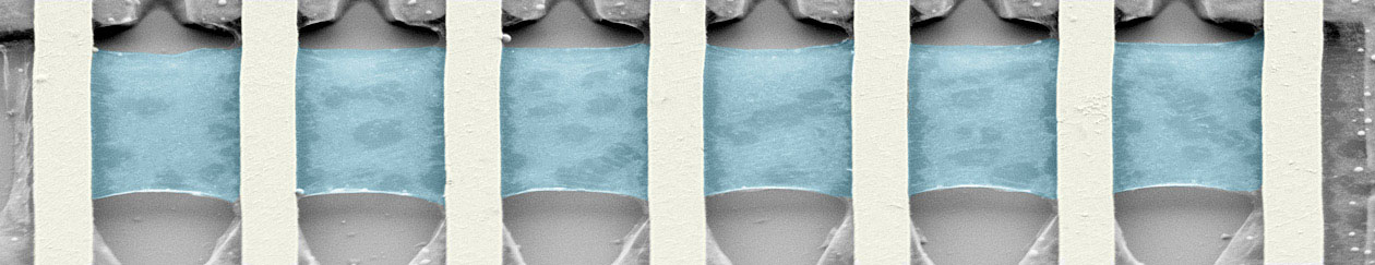
suspended CVD graphene
Master Project: “Circuit QED with RF cavities based on lines with high characteristic impedances” (November 2017)
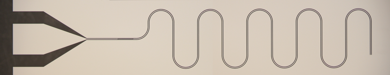
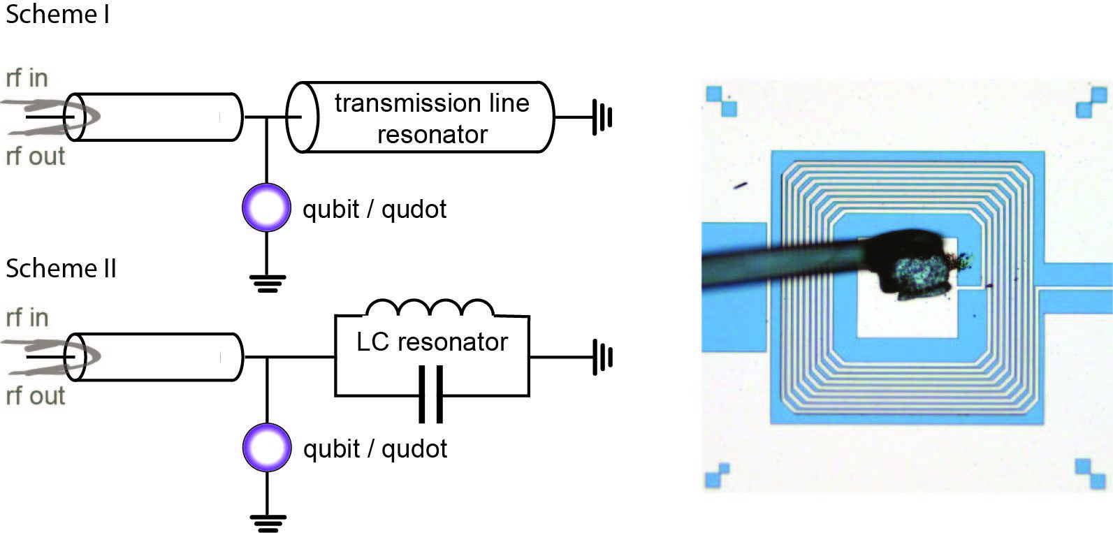
In circuit QED (cQED) a quantum device, such as a quantum dot, for which an effective two-level system can be realized defining a quantum bit (qubit), is coupled to a microwave resonator made e.g. from a transmission line of finite length L, either operated at L=λ/2 in transmission or at L=λ/4 in reflection. cQED has proven to be a very powerful technique. On the one hand, one can use it to read the state of the qubit in an non-demolition manner, if the qubit frequency (determined by the difference in energy between the ground and excited state) is strongly detuned away from the cavity. On the other hand, one can manipulate the qubit with the photons (the microwaves) if the qubit is tuned close to resonance. In order to achieve a fast qubit operation, strong coupling is desirable. This can be achieved by either designing a cavity with a large characteristic impedance using for example a meta-material (e.g. an linear array of superconducting SQUIDs) or a LC resonators with large characteristic impedances.
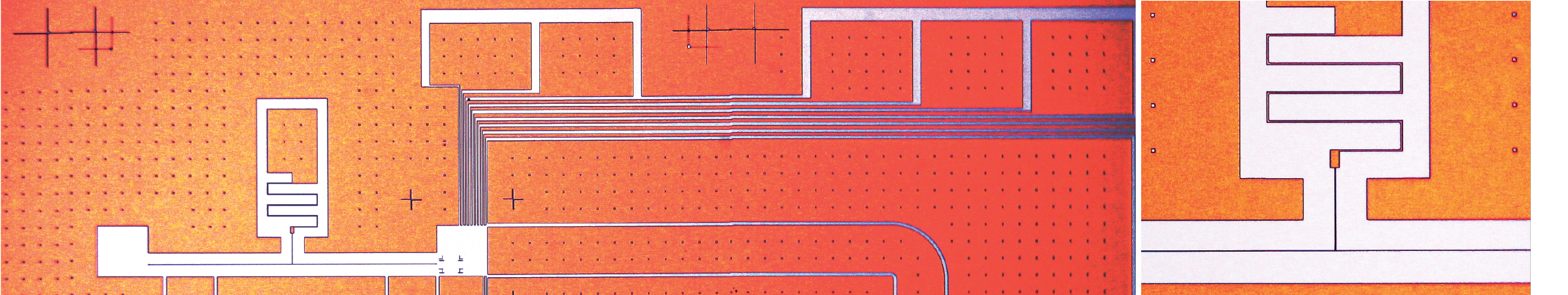
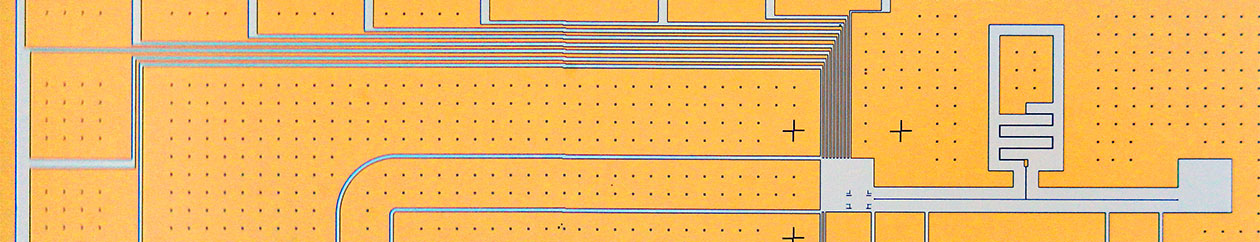
It has been shown recently that the superconductor NbTiN possess many characteristics highly suitable to realize resonators that lead to strong coupling with a very compact footprint, a great advantage if scaling of qubits to a quantum computer is considered. First, NbTiN transmission line resonators have shown to provide high quality factors beyond 100’000, and secondly, due to the large kinetic inductance, the characteristic impedance increases. This increases the electric field in the coupling capacitor to the quibit, potentially leading to strong coupling. Furthermore, a DC current bias through a thin and narrow NbTiN wire allows to tune the inductance, and henceforth the resonance frequency. It also enables parametric amplification.
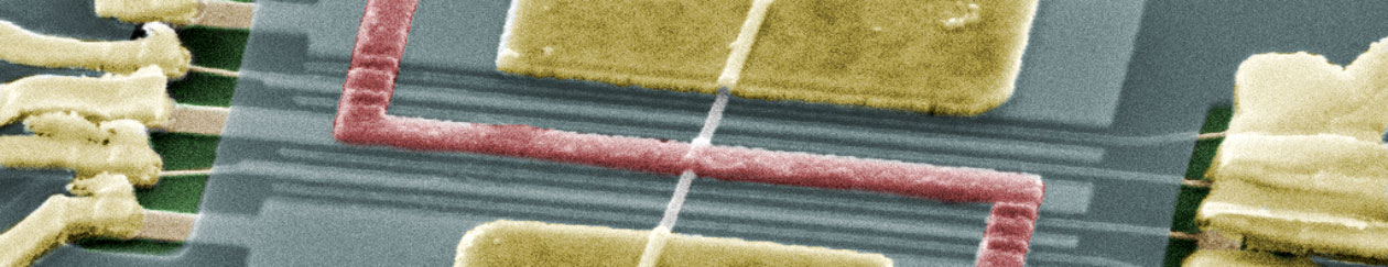
In this project you will fabricated NbTiN films and structure the films into transmission lines, wires and coils that define inductors. You will characterize the properties of these circuit elements (quality factors, resonance frequency) and eventually, you will couple a quantum dot to the circuit that performs best.
To apply, please email to me (Christian.Schoenenberger@unibas.ch) with a short motivation statement.
Christian Schönenberger heads the quantum- & nanoelectronics group, see www.nanoelectronics.ch