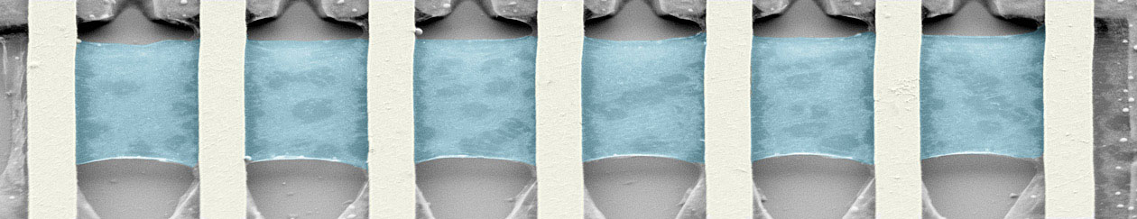
suspended CVD graphene

peter.makk-at-unibas.ch
Phone: +41 61 267 37 03
Education
| 2007-2012 | PhD in Physics at the Budapest University of Technology and Economics |
| 2002-2012 | Physics Curriculum at the Budapest University of Technology and Economics |
Research
hybrid nanostructures from graphene and nanowire devices
List of Publications
https://scholar.google.ch/citations?user=YWTFDgQAAAAJ&hl=en
- Electron wave and quantum optics in graphene
Himadri Chakraborti, Cosimo Gorini, Angelika Knothe, Ming-Hao Liu, Peter Makk, Francois D. Parmentier, David Perconte, Klaus Richter, Preden Roulleau, Christian Schönenberger Benjamin Sacépé, and Wenmin Yang.
Journal of Physics: Condensed Matter 36, 2024.
[arXiv:2401.04233 ] [Abstract
  ]
]
In the last decade, graphene has become an exciting platform for electron optical experiments, in some aspects superior to conventional twodimensional electron gases (2DEGs). A major advantage, besides the ultra-large mobilities, is the fine control over the electrostatics, which gives the possibility of realising gap-less and compact p-n interfaces with high precision. The latter host non-trivial states, e.g. , snake states in moderate magnetic fields, and serve as building blocks of complex electron interferometers. Thanks to the Dirac spectrum and its non-trivial Berry phase, the internal (valley and sublattice) degrees of freedom, and the possibility to tailor the band structure using proximity effects, such interferometers open up a completely new playground based on novel device architectures. In this review, we introduce the theoretical background of graphene electron optics, fabrication methods used to realise electron-optical devices, and techniques for corresponding numerical simulations. Based on this, we give a comprehensive review of ballistic transport experiments and simple building blocks of electron optical devices both in single and bilayer graphene, highlighting the novel physics that is brought in compared to conventional 2DEGs. After describing the different magnetic field regimes in graphene p-n junctions and nanostructures, we conclude by discussing the state of the art in graphene-based Mach-Zender and Fabry-Perot interferometers.
- Boosting proximity spin orbit coupling in graphene/WSe2 heterostructures via hydrostatic pressure
B. Fülöp, A. Márffy, S. Zihlmann, M. Gmitra, E. Tóvári, B. Szentpéteri, M. Kedves, K. Watanabe, T. Taniguchi, J. Fabian, C. Schönenberger, P. Makk, and S. Csonka.
npj 2D Materials and Applications 5, 82, 2021.
[arXiv:2103.13325] [ Open Data  ] [Abstract ]
Van der Waals heterostructures composed of multiple few layer crystals allow the engineering of novel materials with predefined properties. As an example, coupling graphene weakly to materials with large spin orbit coupling (SOC) allows to engineer a sizeable SOC in graphene via proximity effects. The strength of the proximity effect depends on the overlap of the atomic orbitals, therefore, changing the interlayer distance via hydrostatic pressure can be utilized to enhance the interlayer coupling between the layers. In this work, we report measurements on a graphene/WSe2 heterostructure exposed to increasing hydrostatic pressure. A clear transition from weak localization to weak anti-localization is visible as the pressure increases, demonstrating the increase of induced SOC in graphene.
- New method of transport measurements on van der Waals heterostructures under pressure
B. Fülöp, A. Márffy, E. Tóvári, M. Kedves, S. Zihlmann, D. Indolese, Z. Kovács-Krausz, K. Watanabe, T. Taniguchi, C. Schönenberger, Kézsmárki I. P. Makk, and S. Csonka.
J. Apl. Phys. 130, 64303, 2021.
[arXiv:2103.14617] [ Open Data ] [Abstract ]
The interlayer coupling, which has a strong influence on the properties of van der Waals heterostructures, strongly depends on the interlayer distance. Although considerable theoretical interest has been demonstrated, experiments exploiting a variable interlayer coupling on nanocircuits are scarce due to the experimental difficulties. Here, we demonstrate a novel method to tune the interlayer coupling using hydrostatic pressure by incorporating van der Waals heterostructure based nanocircuits in piston-cylinder hydrostatic pressure cells with a dedicated sample holder design. This technique opens the way to conduct transport measurements on nanodevices under pressure using up to 12 contacts without constraints on the sample at the fabrication level. Using transport measurements, we demonstrate that a hexagonal boron nitride capping layer provides a good protection of van der Waals heterostructures from the influence of the pressure medium, and we show experimental evidence of the influence of pressure on the interlayer coupling using weak localization measurements on a transitional metal dichalcogenide/graphene heterostructure.
- Global strain-induced scalar potential in graphene devices
L. Wang, A. Baumgartner, P. Makk, S. Zihlmann, B. S. Varghese, D. I. Indolese, K. Watanabe, T. Taniguchi, and C. Schönenberger.
Comm. Phys. 4, 147, 2021.
[arXiv:2009.03035] [ Open Data ] [Abstract ]
By mechanically distorting a crystal lattice it is possible to engineer the electronic and optical properties of a material. In graphene, one of the major effects of such a distortion is an energy shift of the Dirac point, often described as a scalar potential. We demonstrate how such a scalar potential can be generated systematically over an entire electronic device and how the resulting changes in the graphene work function can be detected in transport experiments. Combined with Raman spectroscopy, we obtain a characteristic scalar potential consistent with recent theoretical estimates. This direct evidence for a scalar potential on a macroscopic scale due to deterministically generated strain in graphene paves the way for engineering the optical and electronic properties of graphene and similar materials by using external strain.
- Out-of-plane corrugations in graphene based van der Waals heterostructures
S. Zihlmann, P. Makk, M. K. Rehmann, L. Wang, M. Kedves, D.Indolese, K. Watanabe, T. Taniguchi, D. M. Zumbühl, and C. Schönenberger.
Phys. Rev. B 102, 195404, 2020.
[arXiv:2004.02690] [ Open Data ] [Abstract ]
Two dimensional materials are usually envisioned as flat, truly 2D layers. However out-of-plane corrugations are inevitably present in these materials. In this manuscript, we show that graphene flakes encapsulated between insulating crystals (hBN, WSe2), although having large mobilities, surprisingly contain out-of-plane corrugations. The height fluctuations of these corrugations are revealed using weak localization measurements in the presence of a static in-plane magnetic field. Due to the random out-of-plane corrugations, the in-plane magnetic field results in a random out-of-plane component to the local graphene plane, which leads to a substantial decrease of the phase coherence time. Atomic force microscope measurements also confirm a long range height modulation present in these crystals. Our results suggest that phase coherent transport experiments relying on purely in-plane magnetic fields in van der Waals heterostructures have to be taken with serious care.
- Compact SQUID realized in a double layer graphene heterostructure
D. I. Indolese, P. Karnatak, A. Kononov, R. Delagrange, R. Haller, L. Wang, P. Makk, K. Watanabe, T. Taniguchi, and C. Schönenberger.
Nano Letters 20, 7129–7135, 2020.
[arXiv:2006.05522] [ Open Data ] [Abstract ]
Two-dimensional systems that host one-dimensional helical states are exciting from the perspective of scalable topological quantum computation when coupled with a superconductor. Graphene is particularly promising for its high electronic quality, versatility in van der Waals heterostructures and its electron and hole-like degenerate 0$th$ Landau level. Here, we study a compact double layer graphene SQUID (superconducting quantum interference device), where the superconducting loop is reduced to the superconducting contacts, connecting two parallel graphene Josephson junctions. Despite the small size of the SQUID, it is fully tunable by independent gate control of the Fermi energies in both layers. Furthermore, both Josephson junctions show a skewed current phase relationship, indicating the presence of superconducting modes with high transparency. In the quantum Hall regime we measure a well defined conductance plateau of 2$e^2/h$ an indicative of counter propagating edge channels in the two layers. Our work opens a way for engineering topological superconductivity by coupling helical edge states, from graphene’s electron-hole degenerate 0$th$ Landau level via superconducting contacts.
- Mobility enhancement in graphene by in situ reduction of random strain fluctuations
L. Wang, P. Makk, S. Zihlmann, A. Baumgartner, D. I. Indolese, K. Watanabe, T. Taniguchi, and C. Schönenberger.
Phys. Rev. Lett. 124, 157701, 2020.
[arXiv:1909.13484] [ Open Data ] [Abstract ]
Microscopic corrugations are ubiquitous in graphene even when placed on atomically flat substrates. These result in random local strain fluctuations limiting the carrier mobility of high quality hBN-supported graphene devices. We present transport measurements in hBN-encapsulated devices where such strain fluctuations can be in situ reduced by increasing the average uniaxial strain. When ∼0.2\% of uniaxial strain is applied to the graphene, an enhancement of the carrier mobility by ∼35\% is observed while the residual doping reduces by ∼39\%. We demonstrate a strong correlation between the mobility and the residual doping, from which we conclude that random local strain fluctuations are the dominant source of disorder limiting the mobility in these devices. Our findings are also supported by Raman spectroscopy measurements.
- Large spatial extension of the zero-energy Yu-Shiba-Rusinov state in magnetic field
Z. Scherübl, G. Fülöp, C. P. Moca, J. Gramich, A. Baumgartner, P. Makk, T. Elalaily, C. Schönenberger, J. Nygard, G. Zaránd, and S. Csonka.
Nature Communications 11, 1834, 2020.
[arXiv:1906.08531] [ Open Data ] [Abstract ]
Various promising qubit concepts have been put forward recently based on engineered superconductor (SC) subgap states like Andreev bound states, Majorana zero modes or the Yu-Shiba-Rusinov (Shiba) states. The coupling of these subgap states via a SC strongly depends on their spatial extension and is an essential next step for future quantum technologies. Here we investigate the spatial extension of a Shiba state in a semiconductor quantum dot coupled to a SC for the first time. With detailed transport measurements and numerical renormalization group calculations we find a remarkable more than 50 nm extension of the zero energy Shiba state, much larger than the one observed in very recent scanning tunneling microscopy (STM) measurements. Moreover, we demonstrate that its spatial extension increases substantially in magnetic field.
- In-situ strain tuning in hBN-encapsulated graphene electronic devices
L. Wang, S. Zihlmann, A. Baumgartner, J. Overbeck, K. Watanabe, T. Taniguchi, P. Makk, and C. Schönenberger.
Nano Letters 19, 4097-4102, 2019.
[arXiv:1904.06737] [ Open Data ] [Abstract ]
Using a simple setup to bend a flexible substrate, we demonstrate deterministic and reproducible in-situ strain tuning of graphene electronic devices. Central to this method is the full hBN encapsulation of graphene, which preserves the exceptional quality of pristine graphene for transport experiments. In addition, the on-substrate approach allows one to exploit strain effects in the full range of possible sample geometries and at the same time guarantees that changes in the gate capacitance remain negligible during the deformation process. We use Raman spectroscopy to spatially map the strain magnitude in devices with two different geometries and demonstrate the possibility to engineer a strain gradient, which is relevant for accessing the valley degree of freedom with pseudo-magnetic fields. Comparing the transport characteristics of a suspended device with those of an on-substrate device, we demonstrate that our new approach does not suffer from the ambiguities encountered in suspended devices
- New generation of Moiré superlattices in doubly aligned hBN/graphene/hBN heterostructures
L. Wang, S. Zihlmann, Ming-Hao Liu, P. Makk, K. Watanabe, T. Taniguchi, A. Baumgartner, and C. Schönenberger.
Nano Letters 19, 2371-2376, 2019.
[arXiv:1812.10031] [Abstract ]
The specific rotational alignment of two-dimensional lattices results in a moiré superlattice with a larger period than the original lattices and allows one to engineer the electronic band structure of such materials. So far, transport signatures of such superlattices have been reported for graphene/hBN and graphene/graphene systems. Here we report moiré superlattices in fully hBN encapsulated graphene with both the top and the bottom hBN aligned to the graphene. In the graphene, two different moiré superlattices form with the top and the bottom hBN, respectively. The overlay of the two superlattices can result in a third superlattice with a period larger than the maximum period (\SI{14}{nm}) in the graphene/hBN system, which we explain in a simple model. This new type of band structure engineering allows one to artificially create an even wider spectrum of electronic properties in two-dimensional materials.
- GHz nanomechanical resonator in an ultraclean suspended graphene p-n junction
Minkyung Jung, P. Rickhaus, S. Zihlmann, A. Eichler, P. Makk, and C. Schönenberger.
Nanoscale 11, 4355, 2019.
[arXiv:1812.06412] [Abstract ]
We demonstrate high-frequency mechanical resonators in ballistic graphene p–n junctions. Fully suspended graphene devices with two bottom gates exhibit ballistic bipolar behavior after current annealing. We determine the graphene mass density and built-in tension for different current annealing steps by comparing the measured mechanical resonant response to a simplified membrane model. We consistently find that after the last annealing step the mass density compares well with the expected density of pure graphene. In a graphene membrane with high built-in tension, but still of macroscopic size with dimensions 3 × 1 micrometer^2, a record resonance frequency of 1.17 GHz is observed after the final current annealing step. We further compare the resonance response measured in the unipolar with the one in the bipolar regime. Remarkably, the resonant signals are strongly enhanced in the bipolar regime. This enhancement is caused in part by the Fabry-Pérot resonances that appear in the bipolar regime and possibly also by the photothermoelectric effect that can be very pronounced in graphene p–n junctions under microwave irradiation.
- Non-equilibrium properties of graphene probed by superconducting tunnel spectroscopy
S. Zihlmann, P. Makk, S. Castillas, J. Gramich, K. Thodkar, S. Caneva, R. Wang, S. Hofmann, and C. Schönenberger.
Phys. Rev. B 99, 75419, 2019.
[arXiv:1811.08746] [Abstract ]
We report on non-equilibrium properties of graphene probed by superconducting tunnel spectroscopy. A hexagonal boron nitride (hBN) tunnel barrier in combination with a superconducting Pb contact is used to extract the local energy distribution function of the quasiparticles in graphene samples in different transport regimes. In the cases where the energy distribution function resembles a Fermi-Dirac distribution, the local electron temperature can directly be accessed. This allows us to study the cooling mechanisms of hot electrons in graphene. In the case of long samples (device length L much larger than the electron-phonon scattering length le−ph), cooling through acoustic phonons is dominant. We find a cross-over from the dirty limit with a power law T3 at low temperature to the clean limit at higher temperatures with a power law T4 and a deformation potential of 13..3 eV. For shorter samples, where L is smaller than le−ph but larger than the electron-electron scattering length le−e, the well-known cooling through electron out-diffusion is found. Interestingly, we find strong indications of an enhanced Lorenz number in graphene. We also find evidence of a non-Fermi-Dirac distribution function, which is a result of non-interacting quasiparticles in very short samples
- Wideband and on-chip excitation for dynamical spin injection into graphene
D. I. Indolese, S. Zihlmann, P. Makk, C. Jünger, K. Thodkar, and C. Schönenberger.
Phys. Rev. Appl. 10, 44053, 2018.
[arXiv:1806.09356] [Abstract ]
Graphene is an ideal material for spin transport as very long spin relaxation times and lengths can be achieved even at room temperature. However, electrical spin injection is challenging due to the conductivity mismatch problem. Spin pumping driven by ferromagnetic resonance is a neat way to circumvent this problem as it produces a pure spin current in the absence of a charge current. Here, we show spin pumping into single layer graphene in micron scale devices. A broadband on-chip RF current line is used to bring micron scale permalloy (Ni80Fe20) pads to ferromagnetic resonance with a magnetic eld tunable resonance condition. At resonance, a spin current is emitted into graphene, which is detected by the inverse spin hall voltage in a close-by platinum electrode. Clear spin current signals are detected down to a power of a few milliwatts over a frequency range of 2 GHz to 8 GHz. This compact device scheme paves the way for more complex device structures and allows the investigation of novel materials.
- Signatures of van Hove singularities probed by the supercurrent in a graphene – hBN superlattice
D. I. Indolese, R. Delagrange, P. Makk, J. R. Wallbank, K. Wanatabe, T. Taniguchi, and C. Schönenberger.
Phys. Rev. Lett. 121, 137701, 2018.
[arXiv:1805.10184] [Abstract ]
The bandstructure of graphene can be strongly modified when it is aligned with its Boron Nitride substrate. A moiré superlattice forms, which manifests itself by the appearance of new Dirac points, accompanied by van Hove singularities. In this work, we present supercurrent measurements in a Josephson junction made from such a graphene superlattice in the long and diffusive transport regime, where the supercurrent depends on the Thouless energy. We can then estimate the specific density of states of the graphene superlattice from the combined measurement of the critical current and the normal state resistance. The result matches with theoretical predictions and highlights the strong increase of the density of states at the van Hove singularities. By measuring the magnetic field dependence of the supercurrent, we find the presence of edge currents at these singularities. We explain it by the reduction of the Fermi velocity associated with the flat band at the van Hove singularity, which suppresses the supercurrent in the bulk while the electrons at the edge remain less localized, resulting in an edge supercurrent. We attribute this different behavior of the edges to defects or chemical doping.
- Co-existence of classical snake states and Aharanov-Bohm oscillations along graphene p-n junctions
Peter Makk, Clevin Handschin, Endre Tovari, Kenji Watanabe, Takashi Taniguchi, Klaus Richter, Ming-Hao Liu, and Christian Schönenberger.
Phys. Rev. B 98, 35413, 2018.
[arXiv:1804.02590] [Abstract ]
Snake states and Aharonov-Bohm interferences are examples of magnetoconductance oscillations that can be observed in a graphene p-n junction. Even though they have already been reported in suspended and encapsulated devices including different geometries, a direct comparison remains challenging as they were observed in separate measurements. Due to the similar experimental signatures of these effects a consistent assignment is difficult, leaving us with an incomplete picture. Here we present measurements on p-n junctions in encapsulated graphene revealing several sets of magnetoconductance oscillations allowing for their direct comparison. We analysed them with respect to their charge carrier density, magnetic field, temperature and bias dependence in order to assign them to either snake states or Aharonov-Bohm oscillations. Furthermore we were able to consistently assign the various Aharonov-Bohm interferences to the corresponding area which the edge states enclose. Surprisingly, we find that snake states and Aharonov-Bohm interferences can co-exist within a limited parameter range
- Large spin relaxation anisotropy and valley-Zeeman spin-orbit coupling in WSe2/Gr/hBN heterostructures
S. Zihlmann, A. W. Cummings, J. H. Garcia, M. Kedves, K. Watanabe, T. Taniguchi, C. Schönenberger, and P. Makk.
Phys. Rev. B 97, 75434, 2018.
[arXiv:1712.05678] [Abstract ]
Large spin-orbital proximity effects have been predicted in graphene interfaced with a transition metal dichalcogenide layer. Whereas clear evidence for an enhanced spin-orbit coupling has been found at large carrier densities, the type of spin-orbit coupling and its relaxation mechanism remained unknown. We show for the first time an increased spin-orbit coupling close to the charge neutrality point in graphene, where topological states are expected to appear. Single layer graphene encapsulated between the transition metal dichalcogenide WSe2 and hBN is found to exhibit exceptional quality with mobilities as high as 100 000 cm2/Vs. At the same time clear weak anti-localization indicates strong spin-orbit coupling and a large spin relaxation anisotropy due to the presence of a dominating symmetric spin-orbit coupling is found. Doping dependent measurements show that the spin relaxation of the in-plane spins is largely dominated by a valley-Zeeman spin-orbit coupling and that the intrinsic spin-orbit coupling plays a minor role in spin relaxation. The strong spin-valley coupling opens new possibilities in exploring spin and valley degree of freedoms in graphene with the realization of new concepts in spin manipulation.
- Spin transport in two-layer-CVD-hBN/graphene/hBN heterostructures
M. Gurram, S. Omar, S. Zihlmann, P. Makk, Q. C. Li, Y. F. Zhang, C. Schönenberger, and B. J. van Wees.
Phys. Rev. B 97, 45411, 2018.
[arXiv:1712.00815] [Abstract ]
We study room-temperature spin transport in graphene devices encapsulated between a layer-by-layer-stacked two-layer-thick chemical vapor deposition (CVD) grown hexagonal boron nitride (hBN) tunnel barrier, and a few-layer-thick exfoliated-hBN substrate. We find mobilities and spin-relaxation times comparable to that of SiO2 substrate-based graphene devices, and we obtain a similar order of magnitude of spin relaxation rates for both the Elliott-Yafet and D’Yakonov-Perel’ mechanisms. The behavior of ferromagnet/two-layer-CVDhBN/ graphene/hBN contacts ranges from transparent to tunneling due to inhomogeneities in the CVD-hBN barriers. Surprisingly, we find both positive and negative spin polarizations for high-resistance two-layer-CVDhBN barrier contacts with respect to the low-resistance contacts. Furthermore, we find that the differential spininjection polarization of the high-resistance contacts can be modulated by dc bias from −0.3 to +0.3 V with no change in its sign, while its magnitude increases at higher negative bias. These features point to the distinctive spin-injection nature of the two-layer-CVD-hBN compared to the bilayer-exfoliated-hBN tunnel barriers.
- Quantum-Confined Stark Effect in a MoS2 Monolayer van der Waals Heterostructure
J. G. Roch, N. Leisgang, G. Froehlicher, P. Makk, K. Watanabe, T. Taniguchi, C. Schönenberger, and R. J. Warburton.
Nano Letters 18, 1070-1074, 2018.
[arXiv:1710.09750] [Abstract ]
The optics of dangling-bond-free van der Waals heterostructures containing transition metal dichalcogenides are dominated by excitons. A crucial property of a confined exciton is the quantum confined Stark effect (QCSE). Here, such a heterostructure is used to probe the QCSE by applying a uniform vertical electric field across a molybdenum disulfide (MoS2) monolayer. The photoluminescence emission energies of the neutral and charged excitons shift quadratically with the applied electric field, provided that the electron density remains constant, demonstrating that the exciton can be polarized. Stark shifts corresponding to about half the homogeneous linewidth were achieved. Neutral and charged exciton polarizabilities of (7.8 +/- 1.0) × 10−10 and (6.4 +/- 0.9) × 10−10 D m V−1 at relatively low electron density (~10^12 cm−2) have been extracted, respectively. These values are one order of magnitude lower than the previously reported values but in line with theoretical calculations. The methodology presented here is versatile and can be applied to other semiconducting layered materials.
- Contactless Microwave Characterization of Encapsulated Graphene p-n Junctions
V. Ranjan, S. Zihlmann, P. Makk, K. Watanabe, T. Taniguchi, and C. Schönenberger.
Phys. Rev. Appl. 7(5), 54015, 2017.
[arXiv:1702.02071] [Abstract ]
Accessing intrinsic properties of a graphene device can be hindered by the influence of contact electrodes. Here, we capacitively couple graphene devices to superconducting resonant circuits and observe clear changes in the resonance-frequency and -widths originating from the internal charge dynamics of graphene. This allows us to extract the density of states and charge relaxation resistance in graphene p-n junctions without the need of electrical contacts. The presented characterizations pave a fast, sensitive and non-invasive measurement of graphene nanocircuits.
- Gate-controlled conductance enhancement from quantum Hall channels along graphene p-n junctions
E. Tovari, P. Makk, Ming-Hao Liu, P. Rickhaus, Z. Kovas-Krausz, C. Schönenberger, and S. Csonka.
Nanoscale 8(47), 19910-19916, 2016.
[arXiv:1606.08007] [Abstract ]
The formation of quantum Hall channels inside the bulk of graphene is studied using various contact and gate geometries. p-n junctions are created along the longitudinal direction of samples, and enhanced conductance is observed in the case of bipolar doping due to the new conducting channels formed in the bulk, whose position, propagating direction and, in one geometry, coupling to electrodes are determined by the gate-controlled filling factor across the device. This effect could be exploited to probe the behavior and interaction of quantum Hall channels protected against uncontrolled scattering at the edges.
- Magnetoresistence engineering and singlet/triplet switching in InAs nanowire quantum dots with ferromagnetic sidegates
G. Fábián, P. Makk, M. H. Madsen, J. Nygård, C. Schönenberger, and A. Baumgartner.
Phy. Rev. B 94, 195415, 2016.
[arXiv:1608.07143] [Abstract ]
We present magnetoresistance (MR) experiments on an InAs nanowire quantum dot device with two ferromagnetic sidegates (FSGs) in a split-gate geometry. The wire segment can be electrically tuned to a single dot or to a double dot regime using the FSGs and a backgate. In both regimes we find a strong MR and a sharp MR switching of up to 25\% at the field at which the magnetizations of the FSGs are inverted by the external field. The sign and amplitude of the MR and the MR switching can both be tuned electrically by the FSGs. In a double dot regime close to pinch-off we find {\it two} sharp transitions in the conductance, reminiscent of tunneling MR (TMR) between two ferromagnetic contacts, with one transition near zero and one at the FSG switching fields. These surprisingly rich characteristics we explain in several simple resonant tunneling models. For example, the TMR-like MR can be understood as a stray-field controlled transition between singlet and a triplet double dot states. Such local magnetic fields are the key elements in various proposals to engineer novel states of matter and may be used for testing electron spin-based Bell inequalities.
- Role of hexagonal boron nitride in protecting ferromagnetic anostructures from oxidation
S. Zihlmann, P. Makk, C. A. F. Vaz, and C. Schönenberger.
2D Materials 3(1), 11008, 2016.
[arXiv:1509.03087] [Abstract ]
Ferromagnetic contacts are widely used to inject spin polarized currents into non-magnetic materials such as semiconductors or 2-dimensional materials like graphene. In these systems, oxidation of the ferromagnetic materials poses an intrinsic limitation on device performance. Here we investigate the role of ex situ transferred chemical vapour deposited hexagonal boron nitride (hBN) as an oxidation barrier for nanostructured cobalt and permalloy electrodes. The chemical state of the ferromagnets was investigated using x-ray photoemission electron microscopy because of its high sensitivity and lateral resolution. We have compared the oxide thickness formed on ferromagnetic nanostructures covered by hBN to uncovered reference structures. Our results show that hBN reduces the oxidation rate of ferromagnetic nanostructures suggesting that it could be used as an ultra-thin protection layer in future spintronic devices.
- Signatures of single quantum dots in graphene nanoribbons within the quantum Hall regime
E. Tovari, P. Makk, P. Rickhaus, C. Schönenberger, and S. Csonka.
Nanoscale 8, 11480, 2016.
[arXiv:1601.01628] [Abstract ]
We report on the observation of periodic conductance oscillations near quantum Hall plateaus in suspended graphene nanoribbons. They are attributed to single quantum dots that form in the narrowest part of the ribbon, in the valleys and hills of a disorder potential. In a wide flake with two gates, a double-dot system’s signature has been observed. Electrostatic confinement is enabled in single-layer graphene due to the gaps that form between Landau levels, suggesting a way to create gate-defined quantum dots that can be accessed with quantum Hall edge states.
- Spin transport in fully hexagonal boron nitride encapsulated graphene
M. Gurram, S. Omar, S. Zihlmann, P. Makk, C. Schönenberger, and B. J. van Wees.
Physical Review B 93(11), 115441, 2016.
[arXiv:1603.04357] [Abstract ]
We study fully hexagonal boron nitride (hBN) encapsulated graphene spin valve devices at room temperature. The device consists of a graphene channel encapsulated between two crystalline hBN flakes: thick-hBN flake as a bottom gate dielectric substrate which masks the charge impurities from Si_{O2}/Si substrate and single-layer thin-hBN flake as a tunnel barrier. Full encapsulation prevents the graphene from coming in contact with any polymer/chemical during the lithography and thus gives homogeneous charge and spin transport properties across different regions of the encapsulated graphene. Further, even with the multiple electrodes in-between the injection and the detection electrodes which are in conductivity mismatch regime, we observe spin transport over 12.5 $\mu$m-long distance under the thin-hBN encapsulated graphene channel, demonstrating the clean interface and the pinhole-free nature of the thin hBN as an efficient tunnel barrier.
- Gate tuneable beamsplitter in ballistic graphene
P. Rickhaus, P. Makk, M. -H. Liu, K. Richter, and C. Schönenberger.
Applied Physics Letters 107, 251901, 2015.
[arXiv:1511.03044] [Abstract ]
We present a beam splitter in a suspended, ballistic, multiterminal, bilayer graphene device. By using local bottomgates, a p-n interface tilted with respect to the current direction can be formed. We show that the p-n interface acts as a semi-transparent mirror in the bipolar regime and that the reflectance and transmittance of the p-n interface can be tuned by the gate voltages. Moreover, by studying the conductance features appearing in magnetic field, we demonstrate that the position of the p-n interface can be moved by 1μm. The herein presented beamsplitter device can form the basis of electron-optic interferometers in graphene
- Gate tuneable beamsplitter in ballistic graphene
P. Makk.
Nature Physics 11, 894-895, 2015.
- Snake trajectories in ultraclean graphene p–n junctions
P. Rickhaus, P. Makk, Ming-Hao Liu, E. Tovari, M. Weiss, R. Maurand, and C. Schönenberger.
Nature Communications 6, 6470, 2015.
[arXiv:1502.01935] [Abstract ]
Snake states are trajectories of charge carriers curving back and forth along an interface. There are two types of snake states, formed by either inverting the magnetic field direction or the charge carrier type at an interface. The former has been demonstrated in GaAs–AlGaAs heterostructures, whereas the latter has become conceivable only with the advance of ballistic graphene where a gap-less p–n interface governed by Klein tunnelling can be formed. Such snake states were hidden in previous experiments due to limited sample quality. Here we report on magneto-conductance oscillations due to snake states in a ballistic suspended graphene p–n junction, which occur already at a very small magnetic field of 20 mT. The visibility of 30 percent is enabled by Klein collimation. Our finding is firmly supported by quantum transport simulations. We demonstrate the high tunability of the device and operate it in different magnetic field regimes.
- Scalable Tight-Binding Model for Graphene
Ming-Hao Liu, P. Rickhaus, P. Makk, E. Tovari, R. Maurand, F. Tkatschenko, M. Weiss, C. Schönenberger, and K. Richter.
Phys. Rev. Lett. 114, 36601, 2015.
[arXiv:1407.5620] [Abstract ]
Artificial graphene consisting of honeycomb lattices other than the atomic layer of carbon has been shown to exhibit electronic properties similar to real graphene. Here, we reverse the argument to show that transport properties of real graphene can be captured by simulations using “theoretical artificial graphene.” To prove this, we first derive a simple condition, along with its restrictions, to achieve band structure invariance for a scalable graphene lattice. We then present transport measurements for an ultraclean suspended single-layer graphene pn junction device, where ballistic transport features from complex Fabry-Pérot interference (at zero magnetic field) to the quantum Hall effect (at unusually low field) are observed and are well reproduced by transport simulations based on properly scaled single-particle tight-binding models. Our findings indicate that transport simulations for graphene can be efficiently performed with a strongly reduced number of atomic sites, allowing for reliable predictions for electric properties of complex graphene devices. We demonstrate the capability of the model by applying it to predict so-far unexplored gate-defined conductance quantization in single-layer graphene.
- Point contacts in encapsulated graphene
C. Handschin, B. Fülöp, P. Makk, S. Blanter, M. Weiss, K. Watanabe, T. Taniguchi, S. Csonka, and C. Schönenberger.
Applied Physics Letters 107(18), 183108, 2015.
[arXiv:1509.04137v1.pdf] [Abstract ]
We present a method to establish inner point contacts on hexagonal boron nitride (hBN) encapsulated graphene heterostructures with dimensions as small as 100 nm by pre-patterning the top-hBN in a separate step prior to dry-stacking. 2 and 4-terminal field effect measurements between different lead combinations are in qualitative agreement with an electrostatic model assuming point-like contacts. The measured contact resistances are 0.5-1.5 k$\Omega$ per contact, which is quite low for such small contacts. By applying a perpendicular magnetic fields, an insulating behaviour in the quantum Hall regime was observed, as expected for inner contacts. The fabricated contacts are compatible with high mobility graphene structures and open up the field for the realization of several electron optical proposals.
- Guiding of Electrons in a Few-Mode Ballistic Graphene Channel
P. Rickhaus, M. -H. Liu, P. Makk, R. Maurand, S. Hess, S. Zihlmann, M. Weiss, K. Richter, and Schönenberger Richter (Uni. C. -. in cooperation with group Regensburg).
Nano Letters 15(5819), 2015.
[arXiv:1509.02653] [Abstract ]
In graphene, the extremely fast charge carriers can be controlled by electron-optical elements, such as waveguides, in which the transmissivity is tuned by the wavelength. In this work, charge carriers are guided in a suspended ballistic few-mode graphene channel, defined by electrostatic gating. By depleting the channel, a reduction of mode number and steps in the conductance are observed, until the channel is completely emptied. The measurements are supported by tight-binding transport calculations including the full electrostatics of the sample.
- Magnetic field tuning and quantum interference in a Cooper pair splitter
G. Fülöp, F. Domínguez, S. d’Hollosy, A. Baumgartner, P. Makk, M. H. Madsen, V. A. Guzenko, J. Nygard, C. Schönenberger, Levy A. Yeyati, Csonka S. -. in cooperation with the Csonka(Budapest), and Levi Yeyati group (Madrid).
Physical Review Letters 115, 227003, 2015.
[arXiv:1507.01036] [Abstract ]
Cooper pair splitting (CPS) is a process in which the electrons of naturally occurring spin-singlet pairs in a superconductor are spatially separated using two quantum dots. Here we investigate the evolution of the conductance correlations in an InAs CPS device in the presence of an external magnetic field. In our experiments the gate dependence of the signal that depends on both quantum dots continuously evolves from a slightly asymmetric Lorentzian to a strongly asymmetric Fano-type resonance with increasing field. These experiments can be understood in a simple three – site model, which shows that the nonlocal CPS leads to symmetric line shapes, while the local transport processes can exhibit an asymmetric shape due to quantum interference. These findings demonstrate that the electrons from a Cooper pair splitter can propagate coherently after their emission from the superconductor and how a magnetic field can be used to optimize the performance of a CPS device. In addition, the model calculations suggest that the estimate of the CPS efficiency in the experiments is a lower bound for the actual efficiency.
- Local electrical tuning of the nonlocal signals in a Cooper pair splitter
G. Fülöp, S. d’Hollosy, A. Baumgartner, P. Makk, V. A. Guzenko, M. H. Madsen, J. Nygård, C. Schönenberger, and S. Csonka.
Physical Review B 90, 235412, 2014.
[arXiv:1409.0818] [Abstract ]
A Cooper pair splitter consists of a central superconducting contact, S, from which electrons are injected into two parallel, spatially separated quantum dots (QDs). This geometry and electron interactions can lead to correlated electrical currents due to the spatial separation of spin-singlet Cooper pairs from S. We present experiments on such a device with a series of bottom gates, which allows for spatially resolved tuning of the tunnel couplings between the QDs and the electrical contacts and between the QDs. Our main findings are gate-induced transitions between positive conductance correlation in the QDs due to Cooper pair splitting and negative correlations due to QD dynamics. Using a semi-classical rate equation model we show that the experimental findings are consistent with in-situ electrical tuning of the local and nonlocal quantum transport processes. In particular, we illustrate how the competition between Cooper pair splitting and local processes can be optimized in such hybrid nanostructures.
- Large-scale fabrication of BN tunnel barriers for graphene spintronics
W. Fu, P. Makk, R. Maurand, M. Bräuninger, and C. Schönenberger.
Journal of Applied Physics 116(20), 74306, 2014.
[arXiv:1407.1439] [Abstract ]
We have fabricated graphene spin-valve devices utilizing scalable materials made from chemical vapor deposition (CVD). Both the spin-transporting graphene and the tunnel barrier material are CVD-grown. The tunnel barrier is realized by Hexagonal boron nitride, used either as a monolayer or bilayer and placed over the graphene. Spin transport experiments were performed using ferromagnetic contacts deposited onto the barrier. We find that spin injection is still greatly suppressed in devices with a monolayer tunneling barrier due to resistance mismatch. This is, however, not the case for devices with bilayer barriers. For those devices, a spin relaxation time of ∼260 ps intrinsic to the CVD graphene material is deduced. This time scale is comparable to those reported for exfoliated graphene, suggesting that this CVD approach is promising for spintronic applications which require scalable materials.
- Fabrication of ballistic suspended graphene with local-gating
R. Maurand, P. Rickhaus, P. Makk, S. Hess, E. Tovari, C. Handschin, M. Weiss, and C. Schönenberger.
Carbon 79, 486-492, 2014.
[arXiv:1409.4751] [Abstract ]
Herein we discuss the fabrication of ballistic suspended graphene nanostructures supplemented with local gating. Using in-situ current annealing, we show that exceptional high mobilities can be obtained in these devices. A detailed description is given of the fabrication of bottom and different top-gate structures, which enable the realization of complex graphene structures. We have studied the basic building block, the p-n junction in detail, where a striking oscillating pattern was observed, which can be traced back to Fabry-Perot oscillations that are localized in the electronic cavities formed by the local gates. Finally we show some examples how the method can be extended to incorporate multi-terminal junctions or shaped graphene. The structures discussed here enable the access to electron-optics experiments in ballistic graphene.
- High-yield fabrication of nm-sized gaps in monolayer CVD graphene
C. Nef, L. Pósa, P. Makk, W. Fu, A. Halbritter, C. Schönenberger, and M. Calame.
Nanoscale 6, 7249-7254, 2014.
[Abstract]
Herein we demonstrate the controlled and reproducible fabrication of sub-5 nm wide gaps in single-layer graphene electrodes. The process is implemented for graphene grown via chemical vapor deposition using an electroburning process at room temperature and in vacuum. A yield of over 95 percent for the gap formation is obtained. This approach allows producing single-layer graphene electrodes for molecular electronics at a large scale. Additionally, from Raman spectroscopy and electroburning carried out simultaneously, we can follow the heating process and infer the temperature at which the gap formation happens.