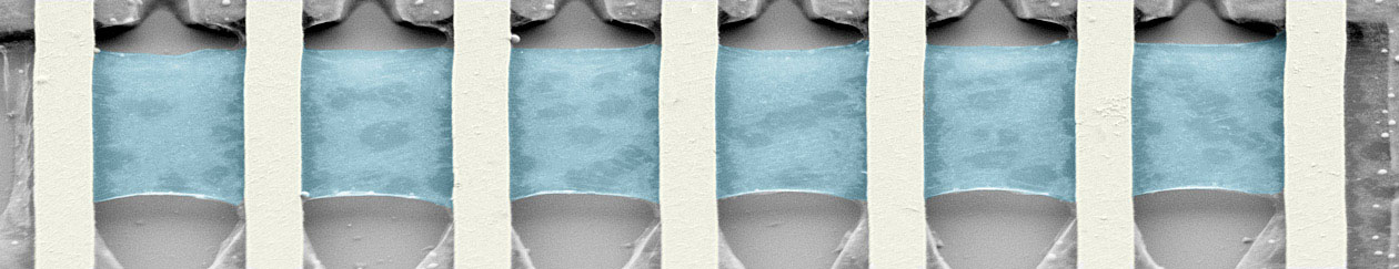
suspended CVD graphene

Preample:
This content of this webpage shows the remnent of the quantum- and nanoelectronics group which was established by Christian Schönenberger in spring 1995 at the University of Basel. It did run till July 2024 when the PI had to retire. The pages with the list of alumni, the PhD theses and publications are still being updated in 2025. However, the description below and details on “ongoing” projects reveal the past.
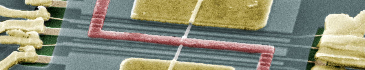
The nanoelectronics group concentrated its research on fundamental electrical properties of engineered nanoscaled devices operating in the quantum regime. We probed these devices by electrical transport measurements both at low (close to DC) and high frequency (GHz range) and at cryogenic temperatures (Kelvin to milli Kelvin). Our devices were based on novel materials with reduced dimensions, either one-dimensional carbon-nanotubes (CNTs), quasi one-dimensional semiconducting nanowires (NWs) or two-dimensional graphene and van der Waals heterostructures which were defined by state-of-art e-beam lithography and complemented with gate and contact electrodes. The group established itself as an internationally recognized leader in so-called hybrid quantum devices that embody in addition to normal metal also superconducting and ferromagnetic electrodes. The latter introduce non-trivial correlations by proximity effect, such as a pairing or exchange field. In combination with intrinsic properties and surface effects, new correlated many-body states can arise. Examples are topological states such as the spin-helix states in one-dimension, molecular Andreev-bound states and Majorana-like states. In addition, we were working on suspended ultraclean van der Waals 2D devices that can additionally be driven mechanically allowing to explore the coupling between mechanical and electrical degrees of freedom at the quantum limit. Another strength of the group were short-noise measurements yielding information complementary to the conductance. The group continued with an intense research activity on 2D van der Waals materials, for example, encapsulated twisted graphene and TMDC devices, which were complemented with superconducting contacts to explore the supercondcuting proximity effect in these 2D materials. In the recent couple of years, the emphasis of the group gradually shifted to qubit research. The group studied charge-, spin- and Andreev qubits as well as gatemon devices realized in semicondcuting nanowires (InAs and GeSi). This later work was also part of the NCCR-Spin.
Research activities / projects (not updated):