suspended CVD graphene
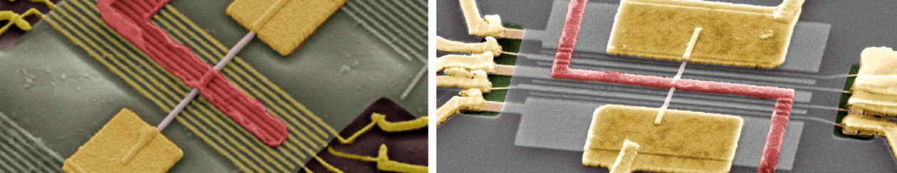
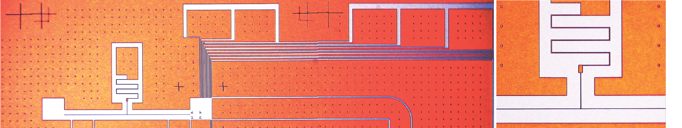
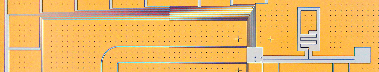
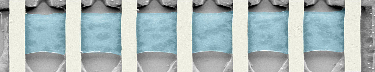
Yet another example of the high quality of h-BN dielectrics that have been engineered and provided by Kenji Watanabe and Takashi Taniguchi from the National Center for Materials Nanoarchitectonics, National Institute for Materials Science, 1-1 Namiki, 17 Tsukuba 305-0044, Japan. The extraordinatory quality of the the dielectric allows to shrink the capacitor that is used as a shunt in the transmon qubit to keep charge noise low. The consequent overall reduction in size enable a better scaling of transmon qubits. Read the News & Views Article by Christian Schoenenberger or the original article: hBN as a low-loss dielectric for superconducting qubits
Highlight hBN dielectrics